Manufacture method and manufacture device for plastic surface-enhancing Raman chip

A technology for surface-enhanced Raman and preparation devices, which is used in measurement devices, Raman scattering, analysis of materials, etc., can solve the problems of complex chemical process, long time, and limit the batch preparation of surface-enhanced chips, and achieves good repeatability and operation. Simple, easy-to-build effects

Inactive Publication Date: 2017-01-11
SHENZHEN UNIV
View PDF3 Cites 2 Cited by
  • Summary
  • Abstract
  • Description
  • Claims
  • Application Information

AI Technical Summary

Problems solved by technology

The chemical processes required by these methods are complicated and time-consuming, which limits the batch preparation of surface-enhanced chips.

Method used


Image

  • Manufacture method and manufacture device for plastic surface-enhancing Raman chip
  • Manufacture method and manufacture device for plastic surface-enhancing Raman chip
  • Manufacture method and manufacture device for plastic surface-enhancing Raman chip

Examples


Embodiment Construction

[0034] In order to make the object, technical solution and advantages of the present invention clearer, the present invention will be further described in detail below in conjunction with the accompanying drawings and embodiments. It should be understood that the specific embodiments described here are only used to explain the present invention, not to limit the present invention.

[0035] The embodiment of the present invention provides a method for preparing a plastic surface enhanced Raman chip, comprising the following steps:

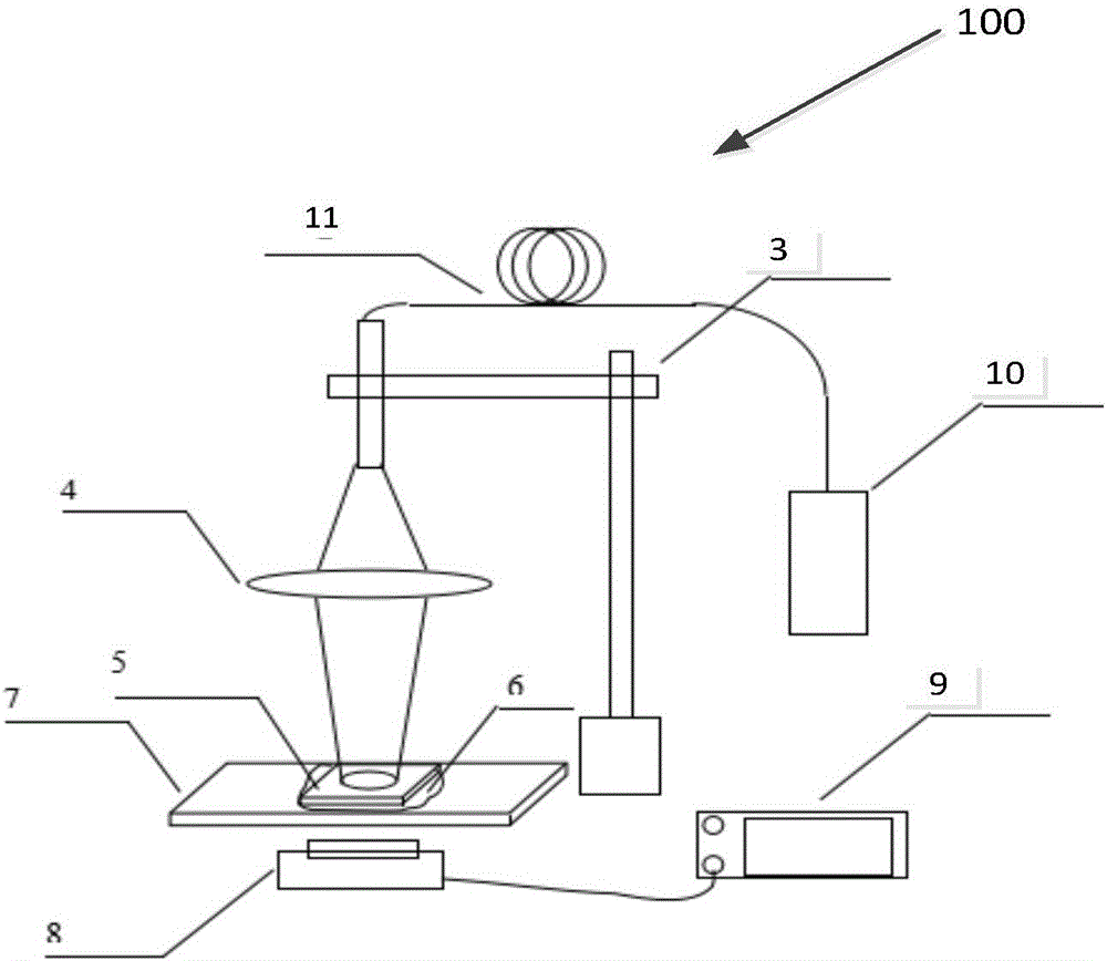
[0036] Generate excitation light and irradiate it on the plastic substrate;

[0037] Dropping the reducing solution onto the surface of the plastic substrate to deposit a layer of metal nanoparticles on the surface of the plastic substrate, and controlling the excitation light power and / or illumination time to make the metal nanoparticles reach the required size;

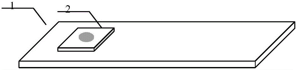
[0038] Remove the reducing solution on the surface of the plastic substrate, and fix...


PUM


Abstract

The invention is applicable to the technical field of Raman scattering, and provides a manufacture method for a plastic surface-enhancing Raman chip. The manufacture method comprises the following steps: exciting light is generated and is radiated on a plastic substrate; reduction liquid is dropped on the surface of the plastic substrate so that a layer of metal nanometer particles is deposited on the surface of the plastic substrate; by controlling the power of the exciting light and / or the radiating time of the exciting light, the metal nanometer particles reach required size; the reduction liquid on the surface of the plastic substrate is removed; and two sides of the plastic substrate are cured through ultraviolet curing adhesive, so that the plastic surface-enhancing Raman chip is obtained. The invention further provides a manufacture device for the plastic surface-enhancing Raman chip. According to the manufacture method for the plastic surface-enhancing Raman chip, the low-cost plastic substrate is utilized; the exciting light is used for radiation; the metal nanometer particles with the required size can be obtained by only controlling the power of the exciting light and / or the radiating time; and the process is simple and feasible and is good in repeatability.

Description

technical field [0001] The invention belongs to the technical field of Raman scattering, and in particular relates to a preparation method and a preparation device of a plastic surface enhanced Raman chip. Background technique [0002] The number, displacement, intensity and shape of the characteristic peaks of the molecular Raman spectrum are all related to the rotation and vibration energy levels of the molecule, and carry the structural information of the molecule. Therefore, the Raman spectrum is regarded as the "fingerprint" of the molecule and is widely used in Molecular structure analysis and molecular recognition. However, the cross section of single molecule Raman scattering is very small (10-30cm 2 ), the Raman scattering intensity is too weak, the sensitivity is low, and it is easily overwhelmed by the fluorescent background. Surface-enhanced Raman scattering refers to the phenomenon that when molecules are adsorbed on the surface of some metal nanostructure sub...

Claims


Application Information

Patent Timeline
IPC IPC(8): C23C18/44C23C18/20C23C18/16G01N21/65
CPCC23C18/1667C23C18/204C23C18/44G01N21/658
Inventor 耿优福李学金殷震谭晓玲洪学明
Owner SHENZHEN UNIV
Why Eureka
Try Eureka