Optical image capturing system

An optical imaging system and imaging surface technology, applied in optics, optical components, instruments, etc., can solve the problems of increased imaging distortion rate, deterioration of peripheral imaging quality, and inability to meet photography requirements, etc.

Active Publication Date: 2017-01-11
ABILITY OPTO ELECTRONICS TECH
View PDF2 Cites 13 Cited by
  • Summary
  • Abstract
  • Description
  • Claims
  • Application Information

AI Technical Summary

Problems solved by technology

However, the optical system designed with a large aperture often faces the situation of producing more aberrations, resulting in the deterioration of the peripheral imaging quality and the difficulty of manufacturing, while the optical system designed with a wide viewing angle will face an increase in the distortion rate of imaging. The advanced optical imaging system can no longer meet the higher-level photography requirements

Method used


Image

  • Optical image capturing system
  • Optical image capturing system
  • Optical image capturing system

Examples


Embodiment approach

[0158] The sum of the focal lengths fp of each lens with positive refractive power in the optical imaging system is ΣPP, and the sum of the focal lengths of each lens with negative refractive power is ΣNP. An embodiment of the optical imaging system of the present invention satisfies the following conditions: <ΣPP≤200; and f4 / ΣPP≤0.85. Preferably, the following conditions may be satisfied: 0<ΣPP≤150; and 0.01≤f4 / ΣPP≤0.7. Therefore, it is helpful to control the focusing ability of the optical imaging system, and properly distribute the positive refractive power of the system to suppress the premature generation of significant aberrations.

[0159] The first lens may have negative refractive power. Therefore, the light-receiving ability of the first lens can be properly adjusted and the viewing angle can be increased.

[0160] The second lens may have positive refractive power. The third lens may have negative refractive power.

[0161]The fourth lens may have positive refra...

no. 1 example

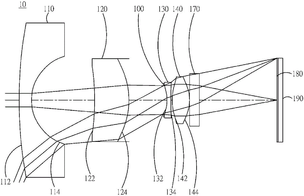
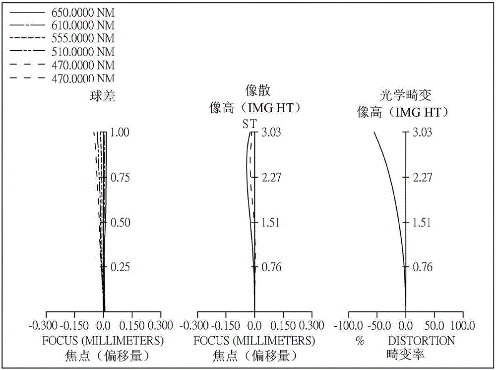
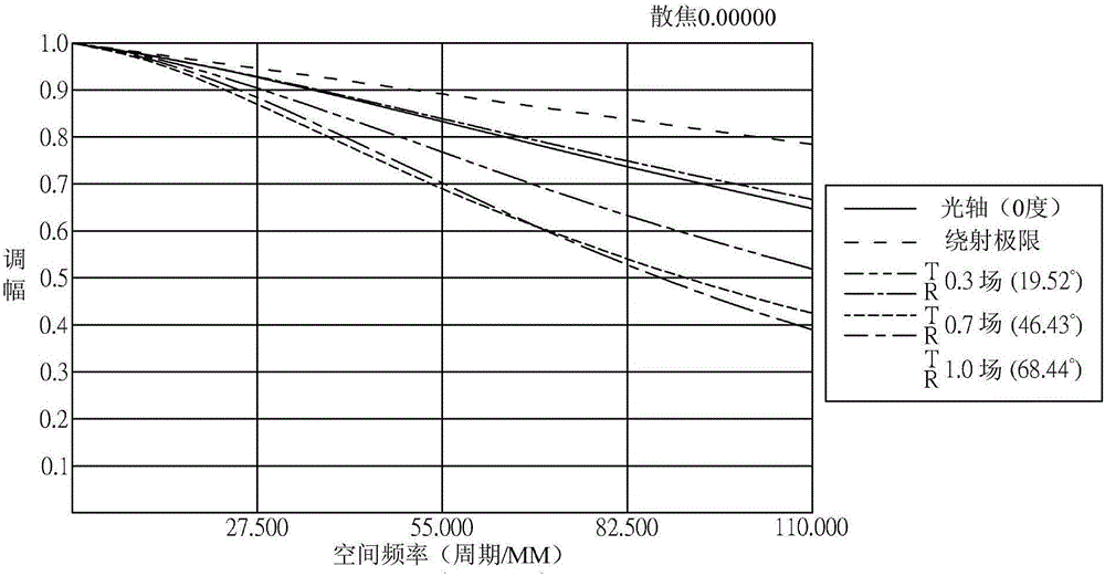
[0193] Please refer to Figure 1A and Figure 1B ,in Figure 1A Representing a schematic diagram of an optical imaging system according to a first embodiment of the present invention, Figure 1B From left to right are the spherical aberration, astigmatism and optical distortion curves of the optical imaging system of the first embodiment. Figure 1C Represents the visible light spectrum modulation conversion characteristic diagram of this embodiment; Figure 1D It shows the infrared spectrum modulation conversion characteristic diagram of this embodiment. Depend on Figure 1A It can be seen that the optical imaging system includes a first lens 110, a second lens 120, an aperture 100, a third lens 130, a fourth lens 140, an infrared filter 170, an imaging surface 180, and an image sensing element from the object side to the image side. 190.

[0194] The first lens 110 has negative refractive power and is made of glass. The object side 112 is convex, and the image side 114 is...

no. 2 example

[0245] Please refer to Figure 2A and Figure 2B ,in Figure 2A A schematic diagram showing an optical imaging system according to a second embodiment of the present invention, Figure 2B From left to right are the spherical aberration, astigmatism and optical distortion curves of the optical imaging system of the second embodiment. Figure 2C Represents the visible light spectrum modulation conversion characteristic diagram of this embodiment; Figure 2D It shows the infrared spectrum modulation conversion characteristic diagram of this embodiment. Depend on Figure 2A It can be seen that the optical imaging system sequentially includes a first lens 210, a second lens 220, an aperture 200, a third lens 230, a fourth lens 240, an infrared filter 270, an imaging surface 280, and an image sensing element from the object side to the image side. 290.

[0246] The first lens 210 has negative refractive power and is made of plastic material. The object side 212 is convex, and ...


PUM


Abstract

An optical image capturing system, sequentially including a first lens element, a second lens element, a third lens element and a fourth lens element from an object side to an image side, is disclosed. The first lens element has negative refractive power, and the object side may be convex. The second through third lens elements have refractive power. Two surfaces of said lenses can be aspheric surfaces. The fourth lens element has positive refractive power, and two surfaces thereof are aspheric surfaces. At least one surface of the fourth lens has an inflection point. The first to fourth lenses of the optical image capturing system have refractive power. If all specific conditions are satisfied, the optical system can increase light gathering and optical path adjusting ability, thus improving the imagining quality.

Description

technical field [0001] The invention relates to an optical imaging system group, and in particular to a miniaturized optical imaging system group applied to electronic products. Background technique [0002] In recent years, with the rise of portable electronic products with photography functions, the demand for optical systems has increased day by day. The photosensitive element of a general optical system is nothing more than a photosensitive coupling device (Charge Coupled Device; CCD) or a complementary metal oxide semiconductor element (Complementary Metal-Oxide Semiconductor duTPor Sensor; CMOS Sensor). The pixel size of components is shrinking, and the optical system is gradually developing into the high-pixel field, so the requirements for image quality are also increasing. [0003] Traditional optical systems mounted on portable devices mostly use two-element or three-element lens structures. However, as portable devices continue to increase the number of pixels an...

Claims


Application Information

Patent Timeline
Patent Type & Authority Applications(China)
IPC IPC(8): G02B13/00G02B13/06G02B13/18
CPCG02B13/004G02B13/06G02B13/18
Inventor 刘耀维张永明
Owner ABILITY OPTO ELECTRONICS TECH
Why Eureka
Try Eureka