Plasma generation device and semiconductor processing device

A technology for generating devices and plasmas, which is applied in semiconductor/solid-state device manufacturing, discharge tubes, electrical components, etc., can solve the problems of increased difficulty in deep silicon etching morphology and roughness control, and reduced process repeatability, achieving Improved reproducibility, easily controlled effects

Active Publication Date: 2017-01-11
BEIJING NAURA MICROELECTRONICS EQUIP CO LTD
View PDF6 Cites 3 Cited by
  • Summary
  • Abstract
  • Description
  • Claims
  • Application Information

AI Technical Summary

Problems solved by technology

This process makes it difficult to control the morphology and roughness of deep

Method used


Image

  • Plasma generation device and semiconductor processing device
  • Plasma generation device and semiconductor processing device
  • Plasma generation device and semiconductor processing device

Examples


Embodiment Construction

[0040] Specific embodiments of the present invention will be described in detail below in conjunction with the accompanying drawings. It should be understood that the specific embodiments described here are only used to illustrate and explain the present invention, and are not intended to limit the present invention.

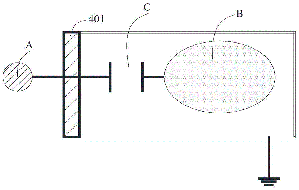
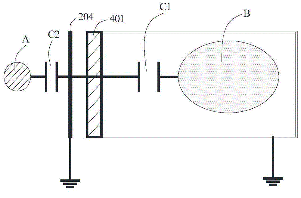
[0041] As an aspect of the present invention, a kind of plasma generating device is provided, such as image 3 and Figure 4 As shown in , the plasma generating device includes a dielectric window 401, an induction coil A arranged around the dielectric window 401 and an impedance matching device, wherein the plasma generating device further includes a dielectric window 401 and an induction coil A arranged between Faraday shield 204 between them.

[0042] It is easy to understand that the space surrounded by the dielectric window 401 is a plasma generation chamber, and a process gas is introduced into the plasma generation chamber during semiconductor processin...


PUM


Abstract

A plasma generation device provided by the present invention comprises a dielectric window, an induction coil surrounding the dielectric window and an impedance matching device, and also comprises a Faraday shielding member arranged between the dielectric window and the induction coil. The present invention also provides a semiconductor processing device. According to the plasma generation device provided by the present invention, the current transmission on the surface of the induction coil is not influenced by the plasma state perturbation any more, so that at work, the plasma generation device provided by the present invention does not generate the phenomena that the plasma quenches, the impedance matching device is matched again, etc., and accordingly, the plasma impedance matching can be realized rapidly, and further the etching morphology of a semiconductor substrate during a Bosch etching technical process is controlled more easily, and the repeatability of the Bosch process is improved.

Description

technical field [0001] The present invention relates to the field of semiconductor processing equipment, in particular to a plasma generating device and a semiconductor processing device including the plasma generating device. Background technique [0002] Currently, a deep silicon etching process is usually used to form a trench with a large aspect ratio on a substrate. A commonly used deep silicon etching process is the Bosch process, which includes alternate etching processes and deposition processes. [0003] In the Bosch process, in order to control the roughness of the sidewall, it is often necessary to quickly switch between the etching gas and the deposition gas, and the parameters such as power and air pressure in the etching process are also related to the power, air pressure and other parameters used in the deposition process. different. Under the influence of the above factors, the plasma impedance in the process chamber often changes greatly. [0004] figure...

Claims


Application Information

Patent Timeline
IPC IPC(8): H01J37/32H01L21/67
Inventor 李兴存赵隆超
Owner BEIJING NAURA MICROELECTRONICS EQUIP CO LTD
Why Eureka
Try Eureka