Method for forming MIS structure

A technology of MIS structure and silicon substrate, which is applied in the fields of electrical components, semiconductor/solid-state device manufacturing, semiconductor devices, etc., can solve the problems of high deposition cost and slow deposition speed of ALD film

Active Publication Date: 2017-01-11
SHANGHAI HUALI MICROELECTRONICS CORP
View PDF4 Cites 0 Cited by
  • Summary
  • Abstract
  • Description
  • Claims
  • Application Information

AI Technical Summary

Problems solved by technology

However, the cost of ALD film deposition is high, the deposition spe

Method used


Image

  • Method for forming MIS structure
  • Method for forming MIS structure
  • Method for forming MIS structure

Examples


Embodiment Construction

[0023] In order to make the content of the present invention clearer and easier to understand, the content of the present invention will be described in detail below in conjunction with specific embodiments and accompanying drawings.

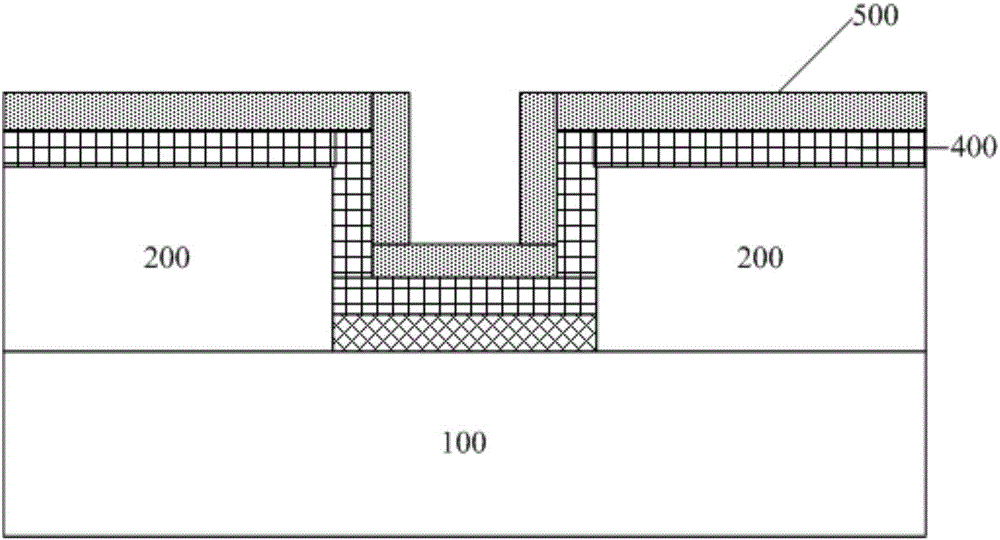
[0024] Figure 1 to Figure 4 Each step of the method for forming the MIS structure according to the preferred embodiment of the present invention is schematically shown.

[0025] Specifically, such as Figure 1 to Figure 4 As shown, the method for forming an MIS structure according to a preferred embodiment of the present invention includes:

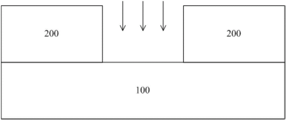
[0026] The first step: performing ion implantation and thermal annealing on the silicon substrate 100 to form an N-type well or a P-type well;

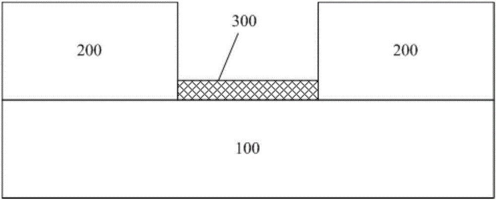
[0027] For example, in the first step, the interlayer dielectric layer pattern 200 is formed on the silicon substrate 100 , and the silicon substrate 100 is ion-implanted and thermally annealed using the interlayer dielectric layer pattern 200 to form an N-type we...


PUM

PropertyMeasurementUnit
Thicknessaaaaaaaaaa
Thicknessaaaaaaaaaa
Thicknessaaaaaaaaaa

Abstract

The invention provides a method for forming an MIS structure. The method includes: step1, performing ion implantation and thermal annealing on a silicon substrate to form an N-type well or a P-type well; step 2, growing a SiO2 layer on the surface of the exposed silicon substrate; step 3, growing a metal Ti layer and a TiN layer on the SiO2 layer in sequence; and step 4, filling tungsten plugs in grooves of the exposed SiO2 layer, and performing planarization processing on the tungsten plugs, the metal Ti layer, and the TiN layer.

Description

technical field [0001] The present invention relates to the field of semiconductor manufacturing, and more specifically, the present invention relates to a method for forming a MIS (metal insulator semiconductor, metal-insulator-semiconductor) structure capable of reducing contact resistance. Background technique [0002] The pinning effect of the Fermi level means that after the metal semiconductor is in contact, a metal-induced splitting energy level will be generated, resulting in a decrease in the probability of electrons breaking through the barrier. When a thin insulating layer is inserted, the induced splitting energy level will be reduced or eliminated, the pinning effect will be eliminated, and the potential barrier will be lowered. [0003] As the size of CMOS shrinks, the requirements for contact resistivity are getting higher and higher, but due to the influence of the Fermi-level pinning effect (Femi-level pinning), it is difficult for the contact resistivity to...

Claims


Application Information

Patent Timeline
IPC IPC(8): H01L21/28
CPCH01L21/28017
Inventor 刘英明
Owner SHANGHAI HUALI MICROELECTRONICS CORP
Why Eureka
Try Eureka