Integrated circuit and self-protection output buffer

An output buffer, integrated circuit technology, applied in circuits, electrical solid devices, electrical components, etc., can solve problems such as large circuit layout area, and achieve the effect of saving layout space, enhancing electrostatic tolerance, and fast turn-on

Inactive Publication Date: 2017-01-11
ADVANCED ANALOG TECH INC
View PDF5 Cites 0 Cited by
  • Summary
  • Abstract
  • Description
  • Claims
  • Application Information

AI Technical Summary

Problems solved by technology

[0004] The purpose of the present invention is to provide a layout structure of an integrated circuit and its output buffer with self-static protection, so as to solve the problem that the output buffer of the general integrated circuit in the prior art takes up too much space due to the addition of an electrostatic protection circuit as an electrostatic protection means. Technical defects in circuit layout area

Method used


Image

  • Integrated circuit and self-protection output buffer
  • Integrated circuit and self-protection output buffer
  • Integrated circuit and self-protection output buffer

Examples


Embodiment Construction

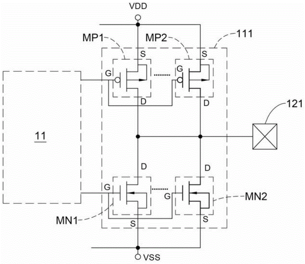
[0066] The present invention improves an output buffer connected to each output pad of an integrated circuit, especially for a large-sized output buffer of a power management integrated circuit, so that the output pad can be directly connected to the output buffer without installing an electrostatic protection circuit, and has the function of self-static protection. The following describes it in detail with several embodiments.

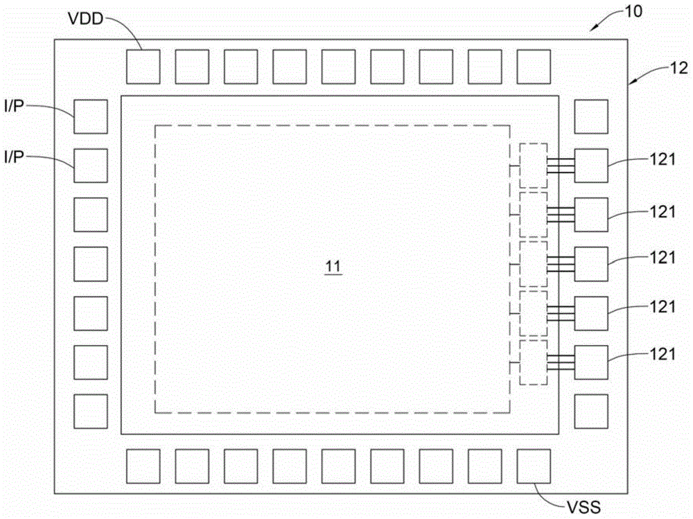
[0067] See first figure 1 as shown, figure 1 It is a schematic layout diagram of an integrated circuit 10 according to the present invention. The integrated circuit 10 includes an internal integrated circuit unit 11 and an input-output ring 12. The input-output ring 12 can surround the internal integrated circuit unit 11, but it is not intended to be To be specific, the input / output ring 12 of this embodiment includes a high potential pad VDD, a low potential pad VSS, a plurality of input pads I / P, a plurality of output pads 121 and the like. The...


PUM


Abstract

Disclosed are an integrated circuit and a self-protection output buffer thereof. The integrated circuit comprises a plurality of output buffers that are connected between a plurality of output pads and an inner integrated circuit unit. Each output buffer comprises a standard MOS element area and an electrostatic protection enhanced MOS element area. The standard MOS element area comprises a plurality of first MOS elements, and the grid electrode areas of the first MOS elements are commonly connected to the inner integrated circuit. The electrostatic protection enhanced MOS element area comprises a plurality of second MOS elements, and the grid electrode areas of the second MOS elements are commonly connected to the inner integrated circuit. The interval between one side of a contact layer of the drain electrode area of each second MOS element and a long side of the nearest polycrystalline silicon area is greater than the interval between one side of a contact layer of the drain electrode area of each first MOS element and a long side of the nearest polycrystalline silicon area. The lower part of the dopant area of the drain area of each second MOS element is provided with a dopant area having different polarity, so that trigger voltage of a gold oxygen hemi-element is reduced, and conduction is accelerated to quickly eliminate static electricity.

Description

technical field [0001] The invention relates to an output buffer of an integrated circuit, in particular to a layout structure of an output buffer with self-static protection. Background technique [0002] Generally speaking, the metal-oxide-semiconductor (MOS) element of an integrated circuit (IC) using a metal-oxide-semiconductor (MOS) process is easily damaged by electrostatic high-voltage discharge . Such as Figure 9 As shown, an internal integrated circuit unit 51 of the integrated circuit 50 is connected to a plurality of output pads 52 (output pads) through a plurality of output buffers 511 (output buffer), and each of the output buffers is composed of MOS elements, That is, it includes PMOS elements (PMOS1~PMOSn) and NMOS elements (NMOS1~NMOSn) (such as Figure 10 shown). Since the output buffer 511 is used to connect to the output pad 52, when static electricity discharges high voltage to the output pad 52, its MOS element is most likely to be damaged by the hig...

Claims


Application Information

Patent Timeline
Patent Type & Authority Applications(China)
IPC IPC(8): H01L27/088H01L27/02H01L23/60
Inventor 林硕彦林欣逸
Owner ADVANCED ANALOG TECH INC
Why Eureka
Try Eureka