Method of forming semiconductor structure

A semiconductor and gate structure technology, applied in the field of semiconductor structure formation, can solve the problems of transistor performance and stability degradation

Active Publication Date: 2017-01-11
SEMICON MFG INT (SHANGHAI) CORP
View PDF3 Cites 2 Cited by
  • Summary
  • Abstract
  • Description
  • Claims
  • Application Information

AI Technical Summary

Problems solved by technology

[0006] However, as the device density in SRAM increases and the size s

Method used


Image

  • Method of forming semiconductor structure
  • Method of forming semiconductor structure
  • Method of forming semiconductor structure

Examples


Embodiment Construction

[0034] As mentioned in the background art, as the device density in the SRAM increases and the size shrinks, the performance and stability of the FinFET in the SRAM also decreases.

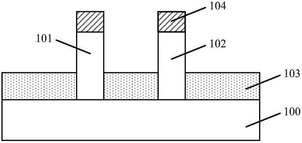
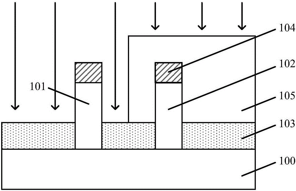
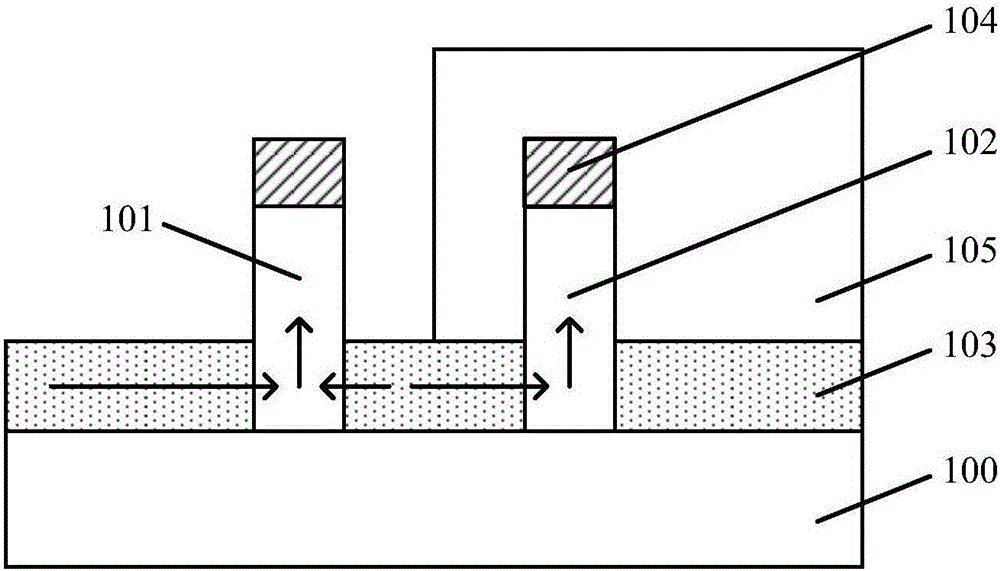
[0035] After research, it is found that as the size of the SRAM decreases and the component density increases, the size of the fin field effect transistor used to form the SRAM also decreases accordingly, and the fin size used to form the fin field effect transistor zoom out. While the size of the fin is reduced, the dopant ions formed in the source region and the drain region in the fin are more likely to diffuse to the bottom region of the fin, and the dopant ions are likely to be short-circuited at the bottom region of the fin, so that The bottom region of the fin causes a punch-through phenomenon, so that the bottom region of the fin easily generates leakage current. Wherein, the bottom area of ​​the fin refers to the area from the position where the fin is flush with the surface of the diele...


PUM


Abstract

The invention provides a method of forming a semiconductor structure. The method comprises steps of providing a substrate, wherein the surface of the substrate has a separating layer, and a first fin part and a second fin part which are adjacent to each other, the surface of the separating layer is lower than the top surfaces of the first fin part and the second fin part, the first fin part comprises a first side wall and a second side wall which are opposite to each other, and the minimal distance from the second side wall to the side wall of the second fin part is smaller than the minimal distance from the first side wall to the side wall of the second fin part; forming a first mask layer on the surfaces of the separating layer, the second fin part and the first fin part, wherein the first mask layer exposes the first side wall of the first fin part and covers a part of the separating layer of the first side wall; taking the first mask layer as a mask layer, and doping first obstruction ions in the separating layer; and carrying out an annealing process to enable the first obstruction ions in the separating layer to be diffused toward the first fin part. The performance of a fin-type field effect transistor formed by the semiconductor structure is improved, and the mismatch problem of the fin-type field effect transistor is reduced.

Description

technical field [0001] The invention relates to the technical field of semiconductor manufacturing, in particular to a method for forming a semiconductor structure. Background technique [0002] Static Random Access Memory (SRAM), as a member of memory, has the advantages of high speed, low power consumption and compatibility with standard processes, and is widely used in computers, personal communications, consumer electronics (smart cards, digital cameras, Multimedia player) and other fields. [0003] The storage unit of the SRAM includes a 4T (transistor) structure and a 6T (transistor) structure. For a 6T SRAM size unit, it includes: a first PMOS transistor P1 , a second PMOS transistor P2 , a first NMOS transistor N1 , a second NMOS transistor N2 , a third NMOS transistor N3 and a fourth NMOS transistor N4 . Wherein, the P1 and P2 are pull-up transistors; the N1 and N2 are pull-down transistors; and the N3 and N4 are transfer transistors. [0004] With the improvemen...

Claims


Application Information

Patent Timeline
IPC IPC(8): H01L29/10H01L21/266
CPCH01L29/66803H01L29/1033H01L21/266
Inventor 周飞
Owner SEMICON MFG INT (SHANGHAI) CORP
Why Eureka
Try Eureka