

Microwave absorbing metamaterial
A technology of metamaterials and absorbing coatings, applied in the field of materials, can solve the problems of narrow absorption electromagnetic wave frequency band, poor tunability of absorbing frequency, etc., and achieve the effect of good absorbing performance and light weight.
- Summary
- Abstract
- Description
- Claims
- Application Information
AI Technical Summary
Problems solved by technology
Method used
Image

Examples
Embodiment 1
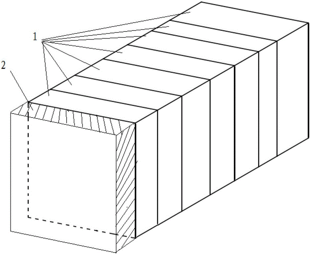
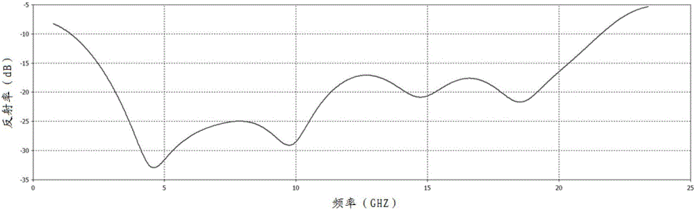
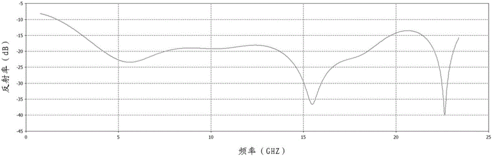
[0032] figure 1 It is a structural schematic diagram of a wave-absorbing metamaterial according to Embodiment 1 of the present invention, such as figure 1 As shown, the microwave-absorbing metamaterial of the present invention includes 7 layers of honeycomb structure layer 1, 7 layers of resistance structure layers (not shown) with a thickness of 0.025mm and a metal plate 2, wherein the metal plate 2 is a copper plate, and the resistance structure layer of the resistance structure layer The area is smaller than the area of the adjacent honeycomb structure layer 1, the resistance structure layer and the honeycomb structure layer 1 are both rectangular, and the lengths of the two are equal. The resistance structure of the resistance structure layer is vertical bars, which are arranged periodically in squares. The 7-layer honeycomb structure layer 1 and the 7-layer resistance structure layer are alternately superimposed on the copper plate. The thickness of the 7-layer honeyco...
Embodiment 2
[0034] The microwave-absorbing metamaterial of the present invention includes 7 layers of honeycomb structure layers, 7 layers of resistance structure layers with a thickness of 0.030mm and a metal plate, wherein the metal plate is an iron plate, and the area of the resistance structure layer is smaller than the area of the adjacent honeycomb structure layer 1 , both the resistance structure layer and the honeycomb structure layer are rectangular, and the widths of the two are equal. The 7-layer honeycomb structure layer and the 7-layer resistance structure layer are alternately superimposed on the copper plate. The thickness of the 7-layer honeycomb structure layer from the outside to the metal plate is: 5.6mm, 5.5mm, 4mm, 5.8mm, 6mm, 6mm, 7.4 mm, the conductivity of the 7-layer resistance structure layer from the outside to the metal plate is: 95S / m, 41S / m, 69S / m, 89S / m, 120S / m, 126S / m and 370S / m, the thickness of the aluminum plate is 0.018mm. The surfaces of the honey...
Embodiment 3
[0036] Such as figure 1 As shown, the microwave-absorbing metamaterial of the present invention includes 7 layers of honeycomb structure layers, 7 layers of resistance structure layers with a thickness of 0.020mm and a metal plate, wherein the metal plate is an aluminum plate, and the 7 layers of honeycomb structure layers and 7 layers of resistance structure layers are sequentially Alternately stacked on the aluminum plate, the area of the resistance structure layer is smaller than the area of the adjacent honeycomb structure layer, the resistance structure layer and the honeycomb structure layer are rectangular, and the width of the two is equal. The thickness of the 7-layer honeycomb structure layer from the outside to the metal plate is: 5.6mm, 5.5mm, 4mm, 5.8mm, 6mm, 6mm, 7mm, and the conductivity of the 7-layer resistance structure layer from the outside to the metal plate is: 95S / m, 35S / m, 69S / m, 89S / m, 120S / m, 126S / m and 694S / m, the thickness of the aluminum plate...
PUM
| Property | Measurement | Unit |
|---|---|---|
| Thickness | aaaaa | aaaaa |
| Thickness | aaaaa | aaaaa |
| Thickness | aaaaa | aaaaa |
Abstract
Description
Claims
Application Information