General chip of printing consumables
A technology for printing consumables and chips, which is applied in the directions of printing, electrical recording process applying charge patterns, equipment for electrical recording technology applying charge patterns, etc. Effect
- Summary
- Abstract
- Description
- Claims
- Application Information
AI Technical Summary
Problems solved by technology
Method used
Image

Examples
Embodiment Construction
[0014] The following will clearly and completely describe the technical solutions in the embodiments of the present invention with reference to the accompanying drawings in the embodiments of the present invention. Obviously, the described embodiments are some of the embodiments of the present invention, but not all of them. Based on the embodiments of the present invention, all other embodiments obtained by persons of ordinary skill in the art without creative efforts fall within the protection scope of the present invention.
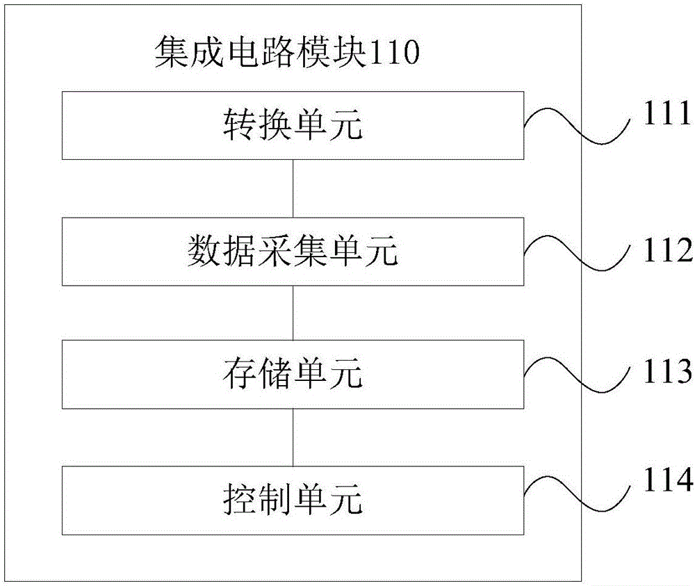
[0015] Such as figure 1 Shown is a schematic structural view of the integrated circuit module of the universal chip of the printing consumables of the present invention. The general-purpose chip includes a substrate provided with contacts and an integrated circuit module, the contacts are electrically connected to the integrated circuit module 110, wherein the integrated circuit module 110 includes:
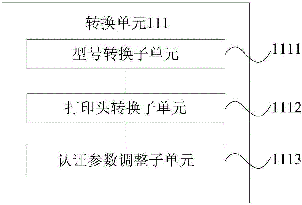
[0016] The conversion unit 111 is configured to re...
PUM
 Abstract
Description
Claims
Application Information
 - R&D
- Intellectual Property
- Life Sciences
- Materials
- Tech Scout
- Unparalleled Data Quality
- Higher Quality Content
- 60% Fewer Hallucinations
Browse by: Latest US Patents, China's latest patents, Technical Efficacy Thesaurus, Application Domain, Technology Topic, Popular Technical Reports.
© 2025 PatSnap. All rights reserved.Legal|Privacy policy|Modern Slavery Act Transparency Statement|Sitemap|About US| Contact US: help@patsnap.com