Method for Junction Staining of Transmission Electron Microscopy Samples

An electron microscope and sample technology, applied in the preparation of test samples, etc., can solve problems such as analysis failures, achieve the effects of improving accuracy and success rate, improving observation quality, and strengthening material contrast

Active Publication Date: 2019-09-17
SHANGHAI HUALI MICROELECTRONICS CORP
View PDF10 Cites 0 Cited by
  • Summary
  • Abstract
  • Description
  • Claims
  • Application Information

AI Technical Summary

Problems solved by technology

This creates a problem where the analysis fails when the defect is located exactly in the cut-out area

Method used


Image

  • Method for Junction Staining of Transmission Electron Microscopy Samples
  • Method for Junction Staining of Transmission Electron Microscopy Samples
  • Method for Junction Staining of Transmission Electron Microscopy Samples

Examples


Embodiment Construction

[0025] In order to make the content of the present invention clearer and easier to understand, the content of the present invention will be described in detail below in conjunction with specific embodiments and accompanying drawings.

[0026] Figure 1 to Figure 15 Each step of the method for staining a transmission electron microscope sample junction according to a preferred embodiment of the present invention is schematically shown.

[0027] like Figure 1 to Figure 15 Shown, according to the method for transmission electron microscope sample junction staining of preferred embodiment of the present invention comprises:

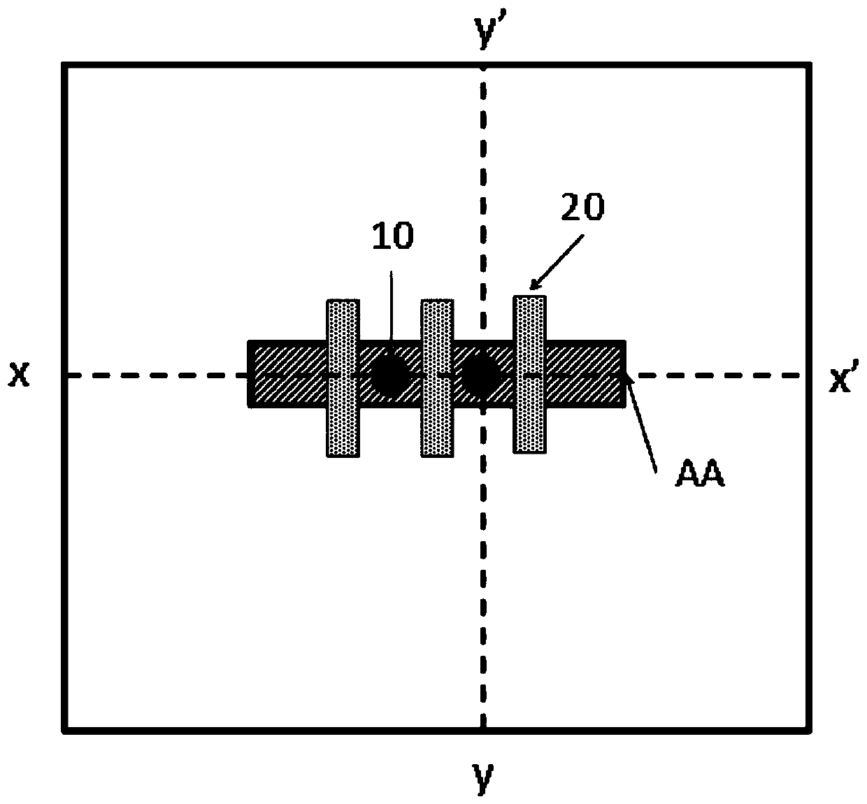
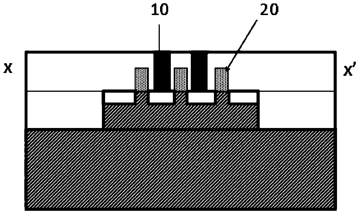
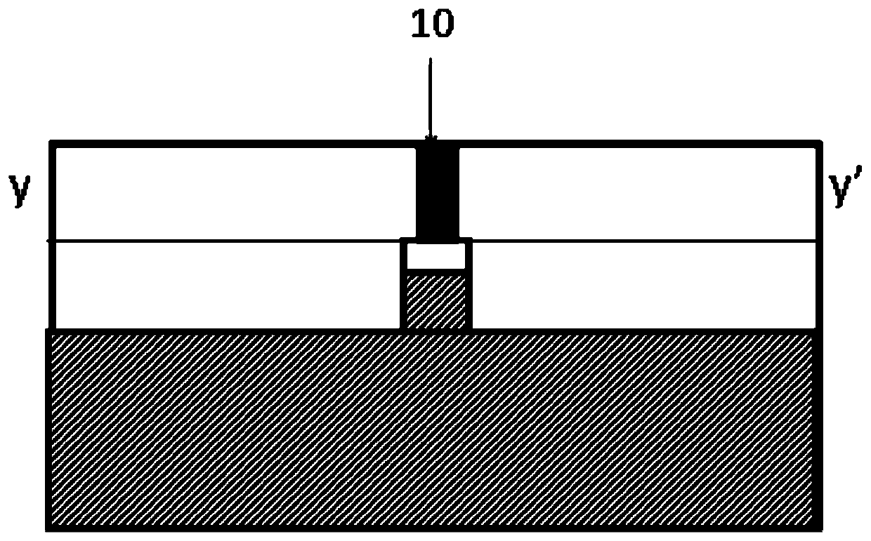
[0028] The first step: processing the chip sample to expose the contact hole 10; for example, polysilicon 20 near the contact hole 10;

[0029] The resulting structure is as figure 1 top view of figure 2 shown along the figure 1 The cross-sectional view taken by the dotted line X-X', and image 3 shown along the figure 1 Shown in the cross-sectional...


PUM

PropertyMeasurementUnit
thicknessaaaaaaaaaa

Abstract

The invention provides a transmission electron microscope sample junction staining method, which comprises the following steps: a chip sample is processed until a contact hole is exposed; a first chemical reagent is used to remove a filler in the contact hole; a second chemical reagent is used to remove doped silicon in a junction below the contact hole; a filling protection layer is deposited on a sample preparation area; and an ion beam is utilized to cut two opposite lateral faces of a transmission electron microscope sample to form transmission electron microscope sample slices, wherein the ion beam doesn't directly cut Si in the sample preparation area but laterally maintains a predetermined thickness of SiO2 from the sample preparation area in allusion to each face.

Description

technical field [0001] The invention relates to the field of integrated circuit analysis, and more specifically, the invention relates to a method for staining a sample of a transmission electron microscope. Background technique [0002] Transmission electron microscopes are widely used in various fields including integrated circuit analysis and are increasingly important, especially in the analysis of tiny defects, which play an irreplaceable role. [0003] There are many kinds of defects that can cause chip failure. Among them, the most difficult to analyze is the very tiny nanoscale doping anomaly. This type of defect cannot be observed by conventional analysis methods such as SEM and transmission electron microscope. At present, the only effective one is Junction staining method using transmission electron microscopy. [0004] The conventional sample preparation process for junction dyeing is to process the plane of the chip sample to be tested close to the target layer...

Claims


Application Information

Patent Timeline
Patent Type & Authority Patents(China)
IPC IPC(8): G01N1/28G01N1/30
Inventor 陈强陈胜
Owner SHANGHAI HUALI MICROELECTRONICS CORP
Why Eureka
Try Eureka