Optical fingerprint sensor

A fingerprint sensor and optical technology, which is applied in the direction of acquiring/arranging fingerprints/palmprints, instruments, character and pattern recognition, etc. It can solve the problems that the structural design of optical fingerprint sensors needs to be improved, and achieve a regular and beautiful appearance, reduce design difficulty, and facilitate assembly. Effect of Difficulty Reduction

Pending Publication Date: 2017-01-18
SHANGHAI OXI TECH
View PDF16 Cites 2 Cited by
  • Summary
  • Abstract
  • Description
  • Claims
  • Application Information

AI Technical Summary

Problems solved by technology

[0005] In the existing optical fingerprint sensor module, the structural design of the optical fingerprint sensor needs to be improved

Method used


Image

  • Optical fingerprint sensor
  • Optical fingerprint sensor
  • Optical fingerprint sensor

Examples


Embodiment Construction

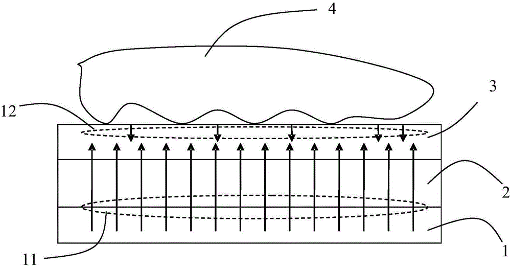
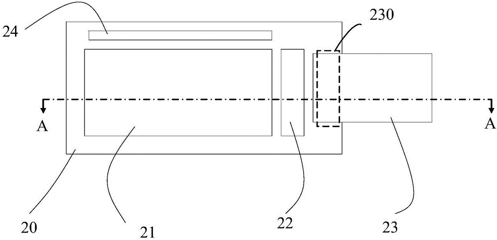
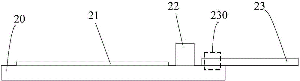
[0035] Please refer to the structure diagram of the existing optical fingerprint sensor figure 2 and image 3 ,in figure 2 is the top view of the optical fingerprint sensor, image 3 for figure 2 The optical fingerprint sensor shown along figure 2 The schematic diagram of the cross-section obtained by cutting the dotted line A-A. The optical fingerprint sensor includes a glass substrate 20 , and a pixel array 21 and peripheral circuits on the glass substrate 20 . The peripheral circuit area includes the driving circuit 24 , the signal readout chip 22 and the flexible printed circuit board 23 . The pixel array 21 is used for receiving, converting and temporarily storing optical signals. The peripheral circuit area also includes the flexible printed circuit board binding area 230, the connection lines between the pixel array 21, the chip 22 and the flexible printed circuit board 23 (each connection line is in the image 3 Not shown in the figure, each connection line ...


PUM


Abstract

The invention discloses an optical fingerprint sensor, which comprises a substrate, a pixel array on the surface of the substrate, a chip on the surface of the substrate, and a flexible printed circuit board bonding region on the surface of the substrate, wherein the pixel array is arranged between the chip and the flexible printed circuit board bonding region. The structural performance of the optical fingerprint sensor is improved.

Description

technical field [0001] The invention relates to the field of optical fingerprint identification, in particular to an optical fingerprint sensor. Background technique [0002] The fingerprint imaging recognition technology is a technology that collects the fingerprint image of the human body through the fingerprint sensor, and then compares it with the existing fingerprint imaging information in the system to judge whether it is correct or not, and then realize the technology of identity recognition. Due to its convenience of use and the uniqueness of human fingerprints, fingerprint recognition technology has been widely used in various fields. For example, security inspection areas such as public security bureaus and customs, building access control systems, and consumer products such as personal computers and mobile phones, etc. The implementation of fingerprint imaging technology includes optical imaging, capacitive imaging, ultrasonic imaging and other technologies. Rel...

Claims


Application Information

Patent Timeline
Patent Type & Authority Applications(China)
IPC IPC(8): G06K9/00
CPCG06V40/1318
Inventor 凌严朱虹
Owner SHANGHAI OXI TECH
Why Eureka
Try Eureka