
PtSi infrared detector for improving quantum efficiency

An infrared detector and quantum efficiency technology, applied in the field of infrared imaging, can solve the problems of low thermal sensitivity and achieve the effects of increasing transmission efficiency, reducing reflection loss, and increasing optical absorption

Inactive Publication Date: 2017-01-18
BEIJING INSTITUTE OF TECHNOLOGYGY
View PDF4 Cites 6 Cited by
  • Summary
  • Abstract
  • Description
  • Claims
  • Application Information

AI Technical Summary

Problems solved by technology

[0006] In view of this, the present invention provides a PtSi infrared detector with improved quantum efficiency, which solves the problem of low thermal sensitivity of traditional detectors due to low quantum efficiency in the mid-wave infrared band (3 μm-5 μm), and improves the detection efficiency. The thermal sensitivity of the device

Method used


Image

  • PtSi infrared detector for improving quantum efficiency
  • PtSi infrared detector for improving quantum efficiency
  • PtSi infrared detector for improving quantum efficiency

Examples


Embodiment

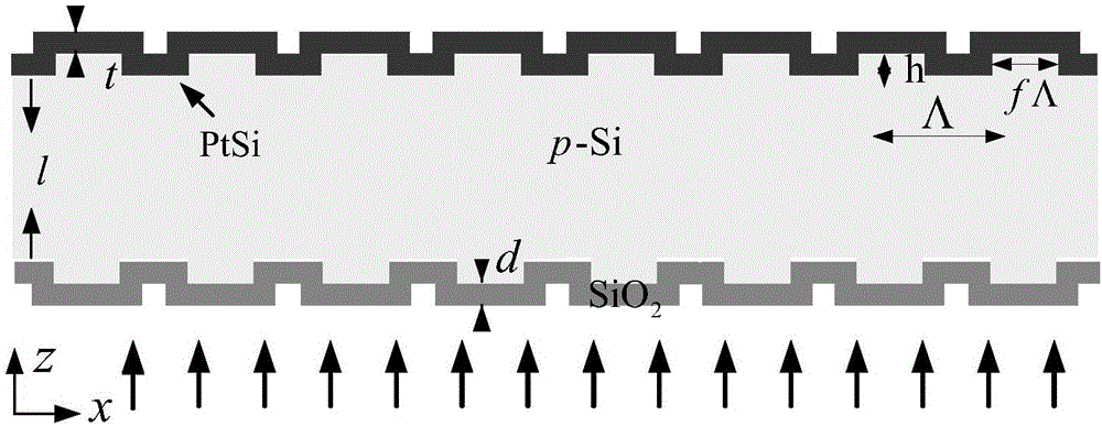
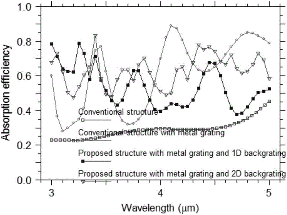
[0029] According to the basic idea above, taking the subwavelength grating anti-reflection structure and metal grating excited PtSi infrared detector as an example, by optimizing the parameters of the subwavelength grating anti-reflection structure and the parameters of the grating-type PtSi metal film, the 3μm- The reflection of the entire band at 5 μm is the smallest, and the PtSi layer absorbs the largest. After a lot of simulations, the grating period Λ, groove depth h, duty cycle f and SiO 2 Anti-reflection film thickness d, basic optimal values ​​of grating period, groove depth, and duty cycle in grating-type PtSi metal film, and then take these optimized values, and then perform local optimization on each of these parameters. Finally, the numerical simulation shows that the period of the sub-wavelength grating anti-reflection structure is 3 μm, the grating groove depth h=0.5 μm, the grating duty cycle f=0.5, SiO 2 Anti-reflection film thickness d=0.4μm, in the grating ...


PUM

PropertyMeasurementUnit
Thicknessaaaaaaaaaa
Grating periodaaaaaaaaaa
Groove depthaaaaaaaaaa

Abstract

The invention discloses a PtSi infrared detector for improving quantum efficiency, belonging to the technical field of infrared imaging. The PtSi infrared detector comprises a p type silicon substrate, a covering grating type PtSi metal film and a silicon dioxide antireflective film. The upper surface of the p type silicon substrate is etched with a grating A, and the lower surface is etched with a grating B. The grating A is a grating structure etched by using a reaction ion dry method, and the surface of the grating A is subjected to the evaporation of Ptsi metal film through a method of magnetron sputtering. The grating B is subwavelength grating structure etched by using a reaction ion dry method, and the surface of the grating B is subjected to the evaporation of a silicon dioxide antireflective film.

Description

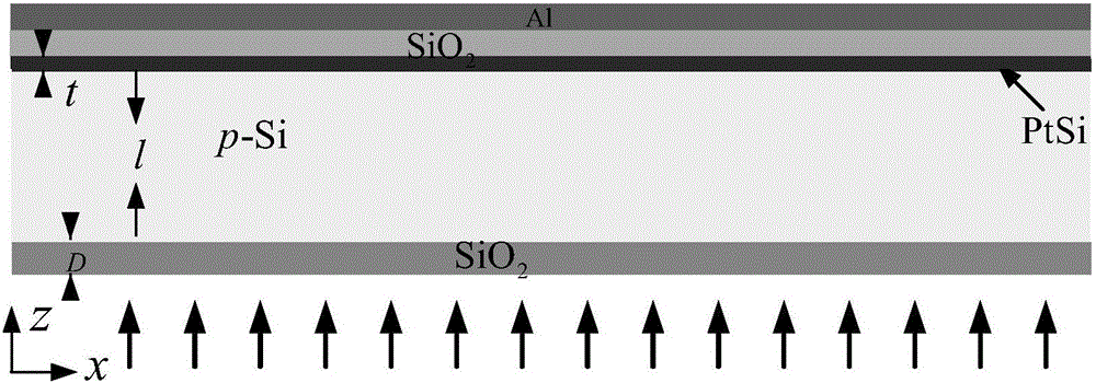
technical field [0001] The invention belongs to the technical field of infrared imaging, and in particular relates to a PtSi infrared detector with improved quantum efficiency. Background technique [0002] Infrared focal plane detector technology is developing in the direction of large area array, wide spectrum, high uniformity, high sensitivity and low cost. [0003] Traditional PtSi infrared detector structure such as figure 1 As shown, it has an aluminum (Al) mirror, a silicon dioxide optical cavity medium, a PtSi metal film (about 3nm), a p-Si substrate (about 450 μm) and a silicon dioxide antireflection film (about 0.8 μm). [0004] Traditional PtSi infrared detector Infrared focal plane detector and CCD readout circuit monolithic integration, at the same time has a large area array, wide spectrum (1μm-10μm), high uniformity (non-uniformity is usually less than 1%), low cost It has attracted attention again because of its application potential in multi-spectral / broad...

Claims


Application Information

Patent Timeline
IPC IPC(8): H01L31/09H01L31/0216
CPCH01L31/09H01L31/0216
Inventor 王岭雪康冰心蔡毅
Owner BEIJING INSTITUTE OF TECHNOLOGYGY
Learn More