How to make the metal grille on the back

A backside metal and manufacturing method technology, applied in the direction of final product manufacturing, sustainable manufacturing/processing, electrical components, etc., can solve problems such as rough side walls of metal grids, avoid high-temperature baking, easy to fall off, and improve yield Effect

Active Publication Date: 2018-06-29
WUHAN XINXIN SEMICON MFG CO LTD
View PDF7 Cites 0 Cited by
  • Summary
  • Abstract
  • Description
  • Claims
  • Application Information

AI Technical Summary

Problems solved by technology

[0009] The invention provides a manufacturing method of the back metal grid to solve the problem of rough side walls of the metal grid formed by the traditional back metal grid manufacturing method

Method used


Image

  • How to make the metal grille on the back
  • How to make the metal grille on the back
  • How to make the metal grille on the back

Examples


Embodiment Construction

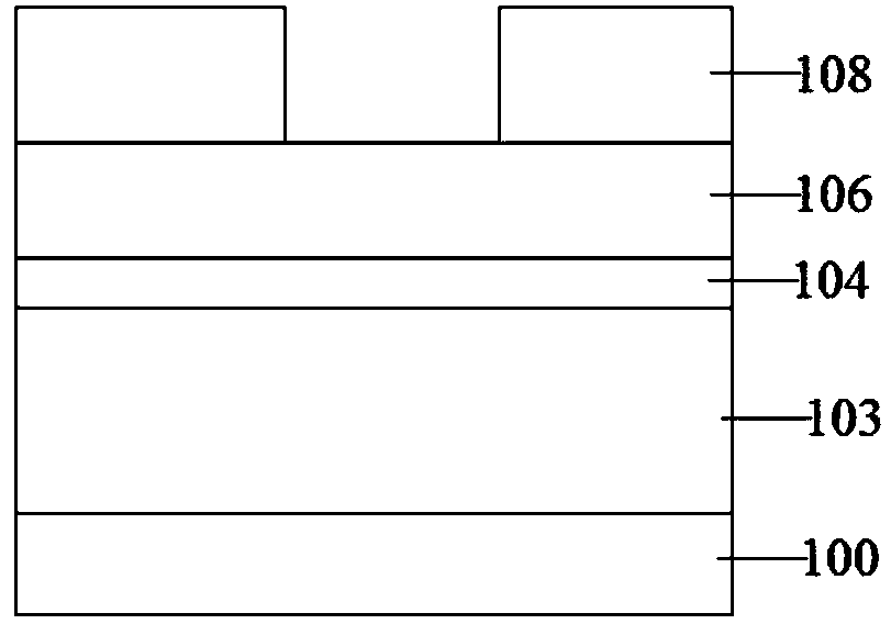
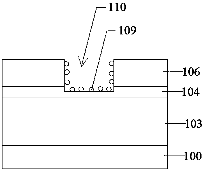
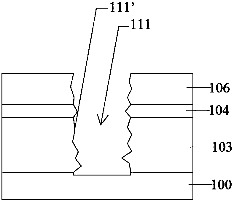
[0050] It has been mentioned in the background art that the sidewalls of the etched metal grid on the semiconductor substrate are so rough that the yield of the semiconductor device is affected by the existing process. After in-depth research, the applicant found that this is due to the formation of a polymer composed of titanium fluoride and carbon-containing compounds in the process of etching the hard mask layer 106 and part of the titanium nitride protective layer 104 with a fluorine-containing gas. 109 (eg figure 2 As shown), the polymer 109 adheres to the bottom and sidewalls of the first trench 110, and it is difficult to completely remove the polymer 109 even after wet cleaning. In this way, when the photoelectric signal transmission layer 103 is subsequently etched, due to the barrier of the polymer 109, the etched sidewall 111' of the second trench is very rough, that is, the sidewall of the metal grid is very rough. , thereby affecting the yield of semiconductor d...


PUM


Abstract

The invention provides a method for fabricating a metal grid on the back, which includes the following steps: providing a semiconductor substrate, and the back of the semiconductor substrate is sequentially formed with a photoelectric signal transmission layer, a titanium nitride protective layer, a hard mask layer and A patterned photoresist layer; using the patterned photoresist layer as a mask, using a fluorine-containing gas to etch the hard mask layer and part of the titanium nitride protective layer; when etching the titanium nitride performing a glue removal process in the cavity of the protective layer; cleaning the semiconductor device; using the hard mask layer as a mask, etching the titanium nitride protective layer and the photoelectric signal transmission layer to form a back surface Metal grille. The invention solves the problem that the side wall of the metal grid formed by the traditional back metal grid manufacturing method is rough.

Description

technical field [0001] The invention relates to the technical field of semiconductor technology, in particular to a method for manufacturing a rear metal grid. Background technique [0002] In semiconductor devices, a backside metal grid (Backside Metal Grid) is usually used as a photoelectric signal transmission channel, which is crucial to the stability of photoelectric signal transmission. [0003] At present, the manufacturing method of the back metal grid in the production process of semiconductor devices includes the following steps: [0004] First, if figure 1 As shown, a photoelectric signal transmission layer 103, a titanium nitride protective layer 104, a hard mask layer 106 and a patterned photoresist layer 108 are sequentially formed on the back of the semiconductor substrate 100; [0005] Next, if figure 2 As shown, using the patterned photoresist layer 108 as a mask, the hard mask layer 106 and part of the titanium nitride protective layer 104 are etched wi...

Claims


Application Information

Patent Timeline
Patent Type & Authority Patents(China)
IPC IPC(8): H01L31/0224H01L31/18
CPCH01L31/0224Y02P70/50
Inventor 谢岩刘选军
Owner WUHAN XINXIN SEMICON MFG CO LTD
Why Eureka
Try Eureka