
A device for real-time measurement of microscopic stress in optical materials based on single crystal dual electro-optic modulation

A technology of electro-optic modulation and micro-stress, applied in the direction of measuring device, measuring force, instrument, etc., can solve the problems of low modulation amplitude, high cost, phase delay interference, etc., and achieve the effect of satisfying real-time observation, improving sensitivity and eliminating interference.

Inactive Publication Date: 2019-09-10
HEBEI UNIV OF TECH
View PDF9 Cites 0 Cited by
  • Summary
  • Abstract
  • Description
  • Claims
  • Application Information

AI Technical Summary

Problems solved by technology

[0008] In view of the above problems, the purpose of the present invention is to propose a device for real-time measurement of the microscopic stress of optical materials based on single crystal dual electro-optical modulation, which solves the interference of thickness fluctuations on the phase delay in the prior art, low precision, insufficient modulation, and high cost. Problems such as low modulation amplitude

Method used


Image

  • A device for real-time measurement of microscopic stress in optical materials based on single crystal dual electro-optic modulation
  • A device for real-time measurement of microscopic stress in optical materials based on single crystal dual electro-optic modulation
  • A device for real-time measurement of microscopic stress in optical materials based on single crystal dual electro-optic modulation

Examples


Embodiment 1

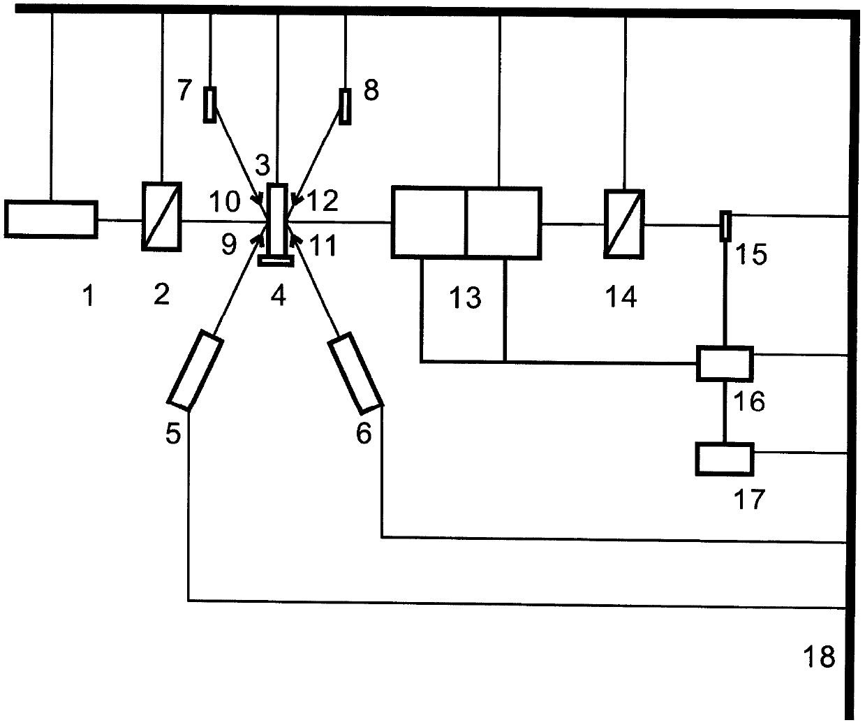
[0083] Design a device based on single crystal dual electro-optic modulation to measure the microscopic stress of optical materials in real time. The extinction ratio of the polarizer and the analyzer is 100000:1, both the polarizer and the analyzer adopt Glan Taylor prisms, the resolution of the electric two-dimensional translation stage is 0.1μm, and the electro-optical modulator has two frequencies ω 1 10kHz, ω 2 It is 30kHz, and the sample is lithium niobate crystal.

Embodiment 2

[0085] Design a device based on single crystal double electro-optic modulation to measure the microscopic stress of optical materials in real time. The extinction ratio of the polarizer and the analyzer is 10000:1, both the polarizer and the analyzer use Glan Taylor prisms, the resolution of the electric two-dimensional translation stage is 0.5μm, and the electro-optical modulator has two frequencies ω 1 1kHz, ω 2 It is 10kHz, and the sample is lithium tantalate crystal.

Embodiment 3

[0087] Design a device based on single crystal double electro-optical modulation to measure the microscopic stress of optical materials in real time. The extinction ratio of the polarizer and the analyzer is 10000:1, the polarizer and the analyzer both use Glan Taylor prisms, the resolution of the electric two-dimensional translation stage is 1 μm, and the electro-optic modulator has two frequencies ω 1 50kHz, ω 2 30kHz, the sample is sapphire crystal.

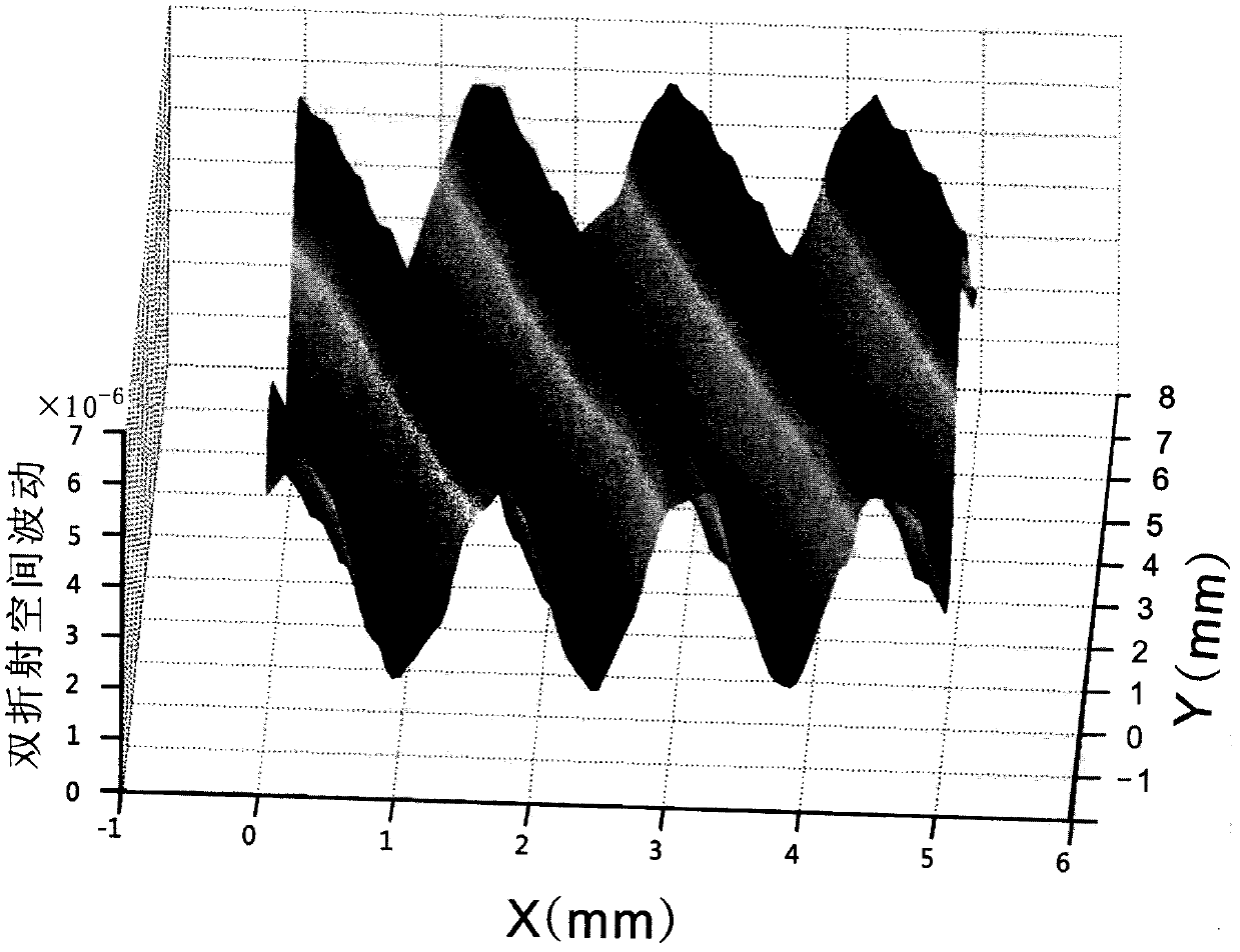
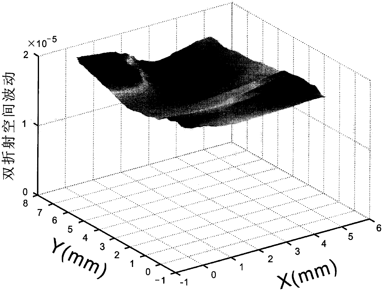
[0088] Utilize detection device of the present invention to carry out microscopic space stress detection (embodiment 1) to lithium niobate crystal, obtain such as Figure 5 The distribution of birefringence spatial fluctuations is shown.


PUM

PropertyMeasurementUnit
wavelengthaaaaaaaaaa

Abstract

The present invention discloses a device and method for real-time measurement of optical material microcosmic stress based on the monocrystal dual-electro-optical modulation, and relates to the microcosmic stress measurement field. The method comprises a first laser, a polarizer, a fine tuning two-dimensional translation table, a second laser, a third laser, a first four quadrant detector, a second four quadrant detector, a dual-electro-optical modulator, an analyzer, a photoelectric detector, a phase locking amplifier and a computer. The device and method for real-time measurement of optical material microcosmic stress based on the monocrystal dual-electro-optical modulation employ the four quadrant detector to perform real-time tracking location measurement of the reflect light of the surface of a test sample and calculate the thickness of the test sample so as to eliminate the interference of the thickness fluctuation for the phase retardation, and employ the monocrystal dual-electro-optical modulation to further improve the measurement precision.

Description

technical field [0001] The invention relates to the technical field of microscopic stress measurement, in particular to a device for real-time measurement of microscopic stress of optical materials based on single crystal dual electro-optical modulation. Background technique [0002] In the process of manufacturing optical crystals in modern industry, the accumulation of optical crystal stress caused by various factors will inevitably occur. The conventional detection technology does not eliminate the interference of the sample thickness fluctuation on the phase delay, so it cannot effectively measure the actual stress of the crystal accurately. Most detection methods use photoelastic modulators to detect samples, which increases the cost of measurement, and the debugging period is long and the operation is inconvenient. [0003] Li Kewu et al. (A device for measuring tiny linear birefringence with elastic-optical modulation and electro-optic modulation coupling, patent app...

Claims


Application Information

Patent Timeline
Patent Type & Authority Patents(China)
IPC IPC(8): G01L1/25
Inventor 阎文博李少北陈洪建陈立品王旭亮樊博麟李菲菲杜城威王晓敏
Owner HEBEI UNIV OF TECH
Learn More