Array substrate, LCD (Liquid Crystal Display) panel and display device

A liquid crystal display panel and array substrate technology, which is applied to semiconductor/solid-state device components, instruments, semiconductor devices, etc., can solve the problems of small increase in the overall aperture ratio of the liquid crystal display panel and small increase in liquid crystal utilization efficiency, and achieve improved Effects of image quality, area reduction, and aperture ratio improvement

Inactive Publication Date: 2017-02-15
BOE TECH GRP CO LTD
View PDF7 Cites 4 Cited by
  • Summary
  • Abstract
  • Description
  • Claims
  • Application Information

AI Technical Summary

Problems solved by technology

[0004] In addition, in order to avoid light leakage at the data lines, the black matrix located above and covering the data lines is usually made wider. In this way, although the width of the black matrix above the gate lines is red

Method used


Image

  • Array substrate, LCD (Liquid Crystal Display) panel and display device
  • Array substrate, LCD (Liquid Crystal Display) panel and display device
  • Array substrate, LCD (Liquid Crystal Display) panel and display device

Examples


Embodiment Construction

[0032] In order to make the purpose of the present invention, technical solutions, and advantages clearer, the present invention will be further described in detail below in conjunction with the accompanying drawings. Obviously, the described embodiments are only some embodiments of the present invention, rather than all embodiments. Based on the embodiments of the present invention, all other embodiments obtained by those skilled in the art without making creative efforts belong to the protection scope of the present invention.

[0033] The specific implementation manners of an array substrate, a liquid crystal display panel, and a display device provided by the embodiments of the present invention will be described in detail below with reference to the accompanying drawings.

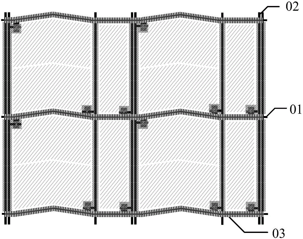
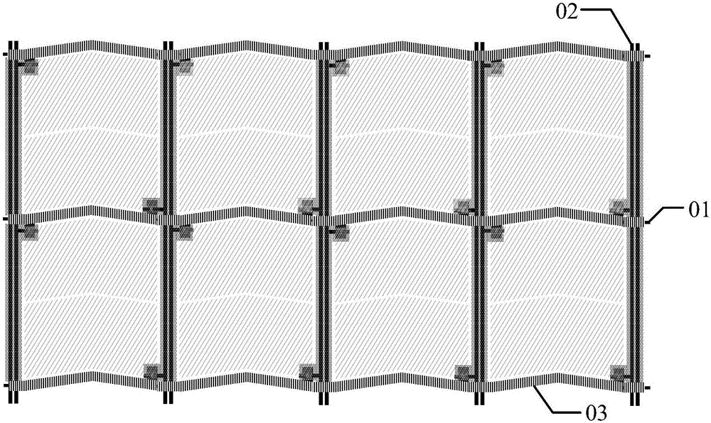
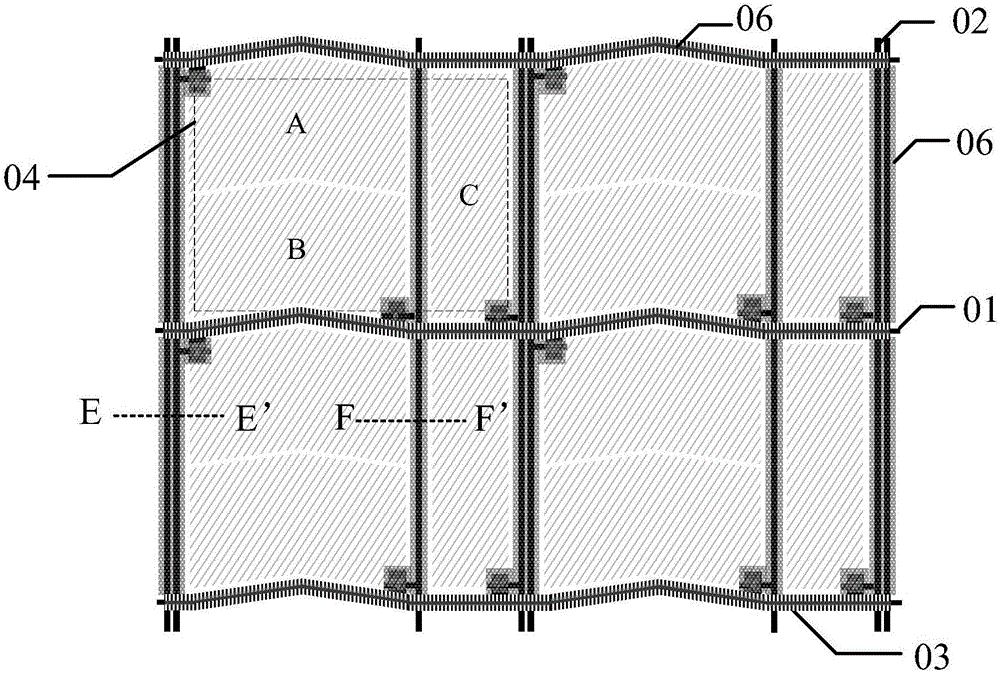
[0034] An embodiment of the present invention provides an array substrate, such as Figure 1a and Figure 1b As shown, it includes: a plurality of gate lines 01 and a plurality of data lines 02 arrange...


PUM


Abstract

The invention discloses an array substrate, an LCD (Liquid Crystal Display) panel and a display device. Under the situation that the numbers of data lines and grid lines are not reduced, two data lines are arranged in a gap between every two adjacent pixel structures through improvement of a data line structure, so that the area of a black matrix for covering the data lines in each pixel structure is reduced to a larger extent, and the aperture opening ratio is increased; meanwhile, through the improvement of the data line structure, the probability that disclination occurs can be further reduced, the utilization rate of liquid crystal is increased, and the transmissivity is further increased; in addition, the grid lines are utilized for shielding, so that the area of the black matrix for covering the grid lines is reduced, the aperture opening ratio and the transmissivity of the LCD panel are greatly increased through combined action of the grid lines and the black matrix, and the image quality of the LCD panel is further greatly increased.

Description

technical field [0001] The invention relates to the field of display technology, in particular to an array substrate, a liquid crystal display panel and a display device. Background technique [0002] In order to meet the development needs of large-scale liquid crystal display panels and wide viewing angles, Advanced Super Dimension Switch (ADS) type liquid crystal display panels came into being. The electric field generated between the slit electrode layer and the plate electrode layer forms a multi-dimensional electric field, so that all oriented liquid crystal molecules between the slit electrodes in the liquid crystal cell and directly above the electrodes can rotate, thereby improving the working efficiency of the liquid crystal and increasing the light transmission. efficiency. [0003] However, when the ADS type liquid crystal display panel is squeezed strongly, due to the displacement of the opposite substrate on the array substrate, if the black matrix above the ga...

Claims


Application Information

Patent Timeline
IPC IPC(8): G02F1/1362
CPCG02F1/136286G02F1/136218G02F1/1362G02F2201/40H01L27/124G02F1/136209G02F1/133512H01L23/5225
Inventor 严允晟
Owner BOE TECH GRP CO LTD
Why Eureka
Try Eureka