Brightness compensation method and device, and display device

A technology of brightness compensation and display equipment, applied in static indicators, instruments, etc., can solve the problems of current changes, affecting OLED brightness, uneven screen display, etc., to achieve uniform brightness, simple design, and low power consumption.

Active Publication Date: 2017-02-15
KUNSHAN GO VISIONOX OPTO ELECTRONICS CO LTD
View PDF10 Cites 21 Cited by
  • Summary
  • Abstract
  • Description
  • Claims
  • Application Information

AI Technical Summary

Problems solved by technology

like figure 2 As shown, the ELVDD voltage is provided to the display panel 30 by the power supply chip through the ELVDD wiring 10, affected by the temperature of the AMOLED display panel 30, the ELVDD wiring impedance R E It will increase with the increase of temperature, so the ELVDD voltage provided to the pixel circuit is affected to cause current changes, affecting the brightness of OLED
In addition, in different positions of the display area, the voltage difference caused by the impedance of the power supply wiring is different, which will cause the overall display of the screen to be uneven.

Method used


Image

  • Brightness compensation method and device, and display device
  • Brightness compensation method and device, and display device
  • Brightness compensation method and device, and display device

Examples


Embodiment Construction

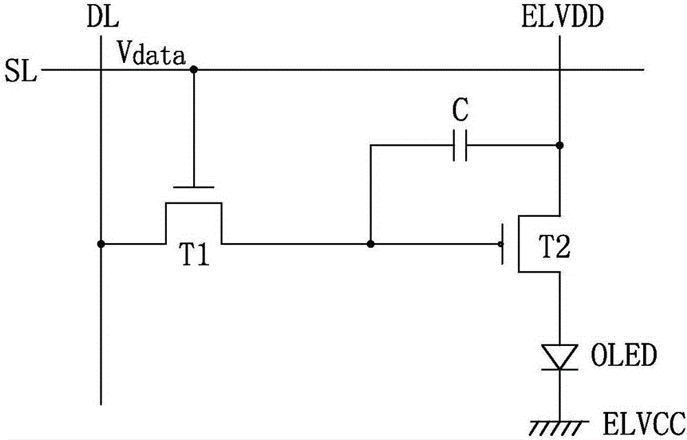
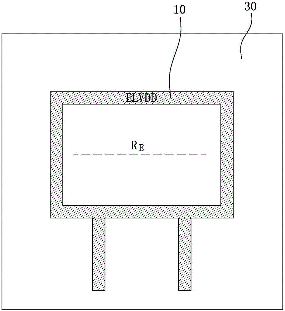
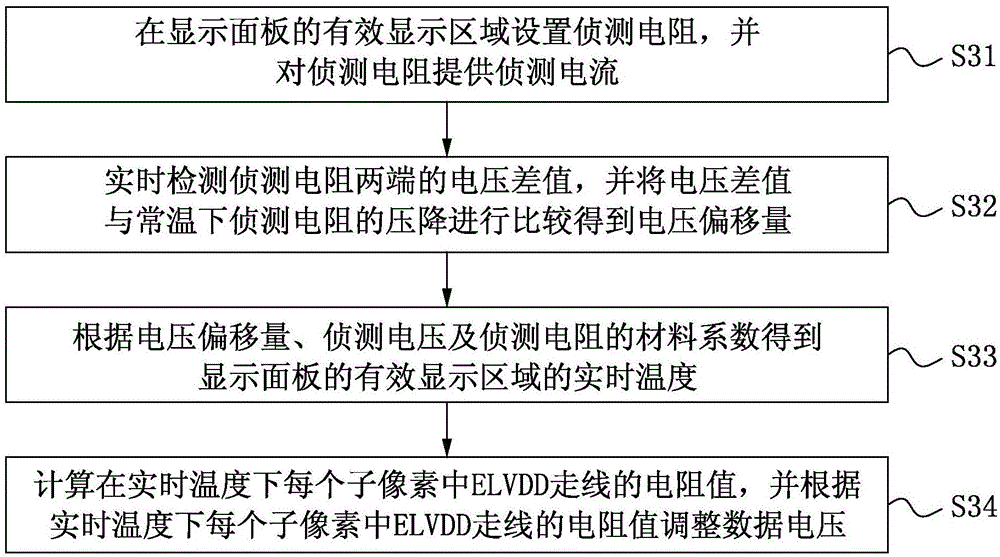
[0015] In order to make the above objects, features and advantages of the present invention more clearly understood, the specific embodiments of the present invention will be described in detail below with reference to the accompanying drawings.

[0016] Although the present invention uses the terms first, second, third, etc. to describe various elements, signals, ports, components or sections, these elements, signals, ports, components or sections are not limited by these terms. These terms are only used to distinguish one element, signal, port, component or section from another element, signal, port, component or section. In the present invention, one element, port, component or part is "connected" or "connected" with another element, port, component or part, which can be understood as a direct electrical connection, or can also be understood as an indirect electrical connection between intermediate elements. sexual connection. Unless otherwise defined, all terms (including...


PUM


Abstract

The invention provides a brightness compensation method. The method comprises: a detection resistor is arranged in an effective display area of a display panel and a detection current is provided for the detection resistor; a voltage difference value of the two ends of the detection resistor is detected in real time and is compared with a voltage drop of the detection resistor at a normal temperature to obtain a voltage offset; according to the voltage offset, the current value of the detection current, and a material coefficient of the detection resistor, a real-time temperature of the effective display area of the display panel is obtained; and a resistance value of ELVDD routing in each sub pixel at a real-time temperature is calculated and a data voltage is adjusted based on the resistance value of the ELVDD routing in each sub pixel at a real-time temperature. In addition, the invention also provides a brightness compensation device and a display device. The real-time temperature of the effective display area can be detected by using the detection resistor arranged in the effective display area and thus the data voltage is adjusted based on the resistance value of the ELVDD routing in each sub pixel. The accuracy is high; the power consumption is low; and the design is simple.

Description

technical field [0001] The present invention relates to the field of display technology, and in particular, to a brightness compensation method, device and display device. Background technique [0002] Active Matrix / Organic Light Emitting Diode (AMOLED) has the advantages of wider viewing angle, higher refresh rate and thinner size, and currently dominates the field of flat panel displays. It is widely used in desktop computers, palmtop computers, personal digital assistants (Personal Digital Assistant, PDA), portable phones, TV boxes and other office automation and audio-visual equipment. [0003] figure 1 It is a schematic structural diagram of a pixel circuit in an existing AMOLED display. like figure 1 As shown, the driving transistor T2 is connected to the organic light emitting diode OLED to provide current for light emission, the switching transistor T1 provides a data voltage to control the current amount of the driving transistor T2, and a capacitor is connected ...

Claims


Application Information

Patent Timeline
Patent Type & Authority Applications(China)
IPC IPC(8): G09G3/3258
CPCG09G3/3258
Inventor 张志华朱修剑葛明伟
Owner KUNSHAN GO VISIONOX OPTO ELECTRONICS CO LTD
Why Eureka
Try Eureka