
Packaging method and packaging body

An encapsulation method and encapsulation technology, which are applied in the manufacturing of electrical solid-state devices, semiconductor devices, and semiconductor/solid-state devices, etc., can solve the problems of overflowing glue, affecting product performance, and difficult to control frame deformation, so as to improve the arrangement density and improve the Service life, the effect of solving operational difficulties

Inactive Publication Date: 2017-02-15
DIODES SHANGHAI +2
View PDF10 Cites 0 Cited by
  • Summary
  • Abstract
  • Description
  • Claims
  • Application Information

AI Technical Summary

Problems solved by technology

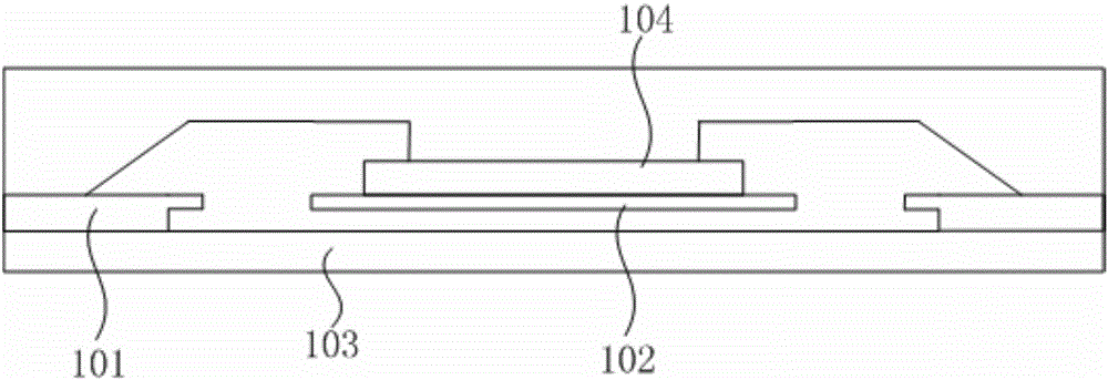
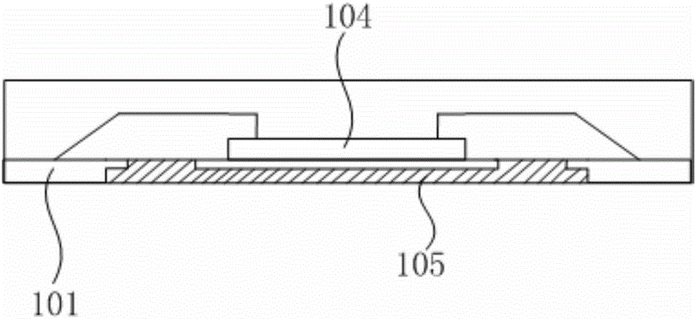
[0004] However, the above method has certain limitations. When the thickness of the frame is very thin, the space for accommodating the glue is small, the frame will be deformed, the glue will overflow, and the yield rate of the pre-injection glue process will be greatly lost, and the frame deformation is difficult to control. , the thinner the frame, the more deformation will occur during the manufacturing process, and the glue overflow situation is very serious
Spilled glue may spread to the pins, affecting the performance of the product

Method used


Image

  • Packaging method and packaging body
  • Packaging method and packaging body
  • Packaging method and packaging body

Examples


no. 2 Embodiment approach

[0047] The packaging method of the present invention also provides a second specific embodiment, the difference between the second specific embodiment and the first specific embodiment is that the materials used to form the pre-filled layer are different. In a second specific implementation manner, the material forming the pre-fill layer is liquid photo-soldering resist. The steps of the second specific embodiment are as follows.

[0048] The method for forming the welding pad in the second embodiment is the same as that in the first embodiment, please refer to the above description and attached Figures 4A-4B . For the method of forming the pre-filled layer, please refer to the following steps.

[0049] See step S60 and Figure 7A1. Coating a pre-fill layer 702 on the surface of the carrier 400 and the welding pad 401, the material of the pre-fill layer 702 is liquid photo-solder resist, and the liquid photo-solder resist is commonly known as green paint. In this specific...


PUM


Abstract

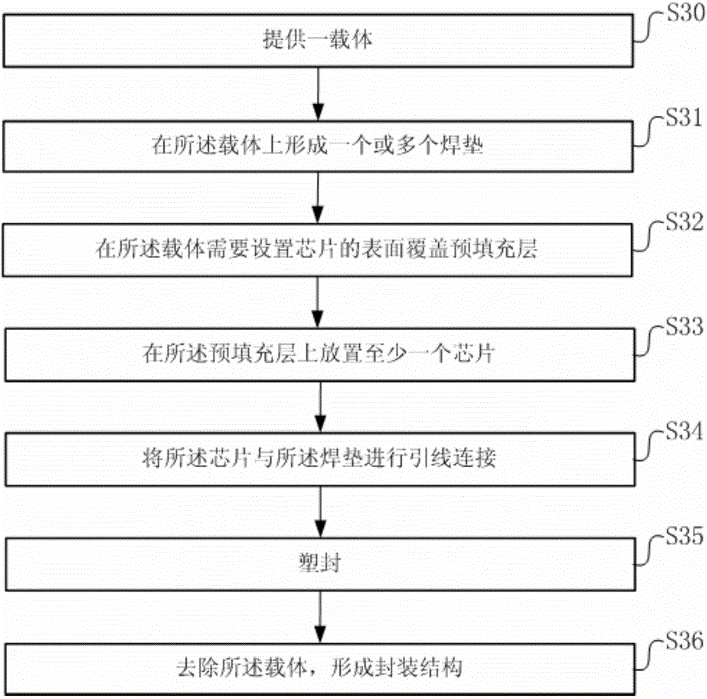
The present invention provides a packaging method and a packaging body. The packaging method comprises a step of providing a carrier, a step of forming one or more pads on the carrier, a step of covering the surface of the carrier with the need of arranging a chip with a pre-filling layer, a step of placing at least one chip on the pre-filling layer, a step of carrying out lead connection of the chip and the pads, and a step of carrying out plastic packaging and removing the carrier to form a package structure. The packaging method and the packaging body have the advantages that the problem of putting a welding line to a chip suspended island can be solved, thus the welding line has good operation, the layout density can be improved, the service life of a cutting knife can be improved, thus the cost is saved, a thinner package body can be obtained, and a series of operating difficulties of a super thin substrate caused by low intensity in the production process is solved.

Description

technical field [0001] The invention relates to the field of semiconductor packaging, in particular to a packaging method and a packaging body. Background technique [0002] Some existing packaging products, such as QFN products, may have no exposed chip pads (exposed pads) or products with chip pads (exposed pads) that are very small. see figure 1 , the frame includes pins 101 and base island 102, the pins 101 are attached to the pre-adhesive film 103, and the pre-adhesive film 103 plays a supporting role, and since there is no exposed heat sink, the frame is half in the area where the chip is placed. Etching design, that is, the base island 102 is half-etched, and the chip 104 is placed on the base island 102. In this way, the wire bonding area on the chip 104 is in a suspended state, resulting in the inability to wire wire or the difficulty of wire bonding, and the workability of the wire bonding. not good. [0003] In the prior art, the method to solve this problem is...

Claims


Application Information

Patent Timeline
Patent Type & Authority Applications(China)
IPC IPC(8): H01L21/56H01L21/60H01L23/31
CPCH01L21/568H01L23/3121H01L24/85H01L2224/85005H01L2224/48247H01L2224/73265H01L2224/97H01L2924/181H01L2924/00012
Inventor 阳小芮刘道健
Owner DIODES SHANGHAI
Learn More