Zero-tolerance depth-controllable drilling method for circuit board

A drilling method and circuit board technology, which are applied in the directions of printed circuits, printed circuit manufacturing, and the formation of electrical connection of printed components, can solve the problems of small design aperture accuracy, limited angle of ordinary drill tip, and insufficient flatness of drilling rigs. Guarantee quality and reliability, meet the needs of the effect

Inactive Publication Date: 2017-02-15
SHENZHEN SUNTAK MULTILAYER PCB
View PDF4 Cites 10 Cited by
  • Summary
  • Abstract
  • Description
  • Claims
  • Application Information

AI Technical Summary

Problems solved by technology

[0003] For High Power Density Inverter (HDI) boards, which use more blind or buried hole technology, with higher circuit density, with the gradual development of HDI boards, the design is more complex, the aperture is smaller, and the accuracy is higher. Higher, ordinary laser drilling or mechanical drilling is difficult to meet the depth requirements of the hole, especially for low-loss microwave products, which require extremely accurate hole depth accuracy. For blind or buried holes with limited hole depth, mechanical depth control can be used Drilling rig production, but the existing mechanical depth control drilling rig has insufficient flatness of the drilling machine and the limited angle of the ordinary drill tip, so that the mechanical control depth drilling rig cannot accurately control the drilling depth to reach the target level, and the existence of this tolerance will also affect the signal It has a great negative impact on the transmission of printed circuit boards and cannot meet the increasingly stringent requirements for printed circuit boards. Obviously, the smaller the tolerance, the less signal loss and the smaller the impact on the signal transmission of the circuit board. Therefore, the development of a zero Tolerance controlled depth drilling technology is the general trend

Method used


Image

  • Zero-tolerance depth-controllable drilling method for circuit board
  • Zero-tolerance depth-controllable drilling method for circuit board
  • Zero-tolerance depth-controllable drilling method for circuit board

Examples


Embodiment

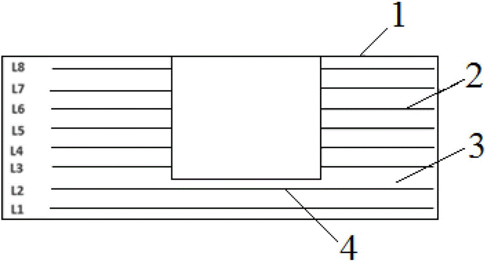
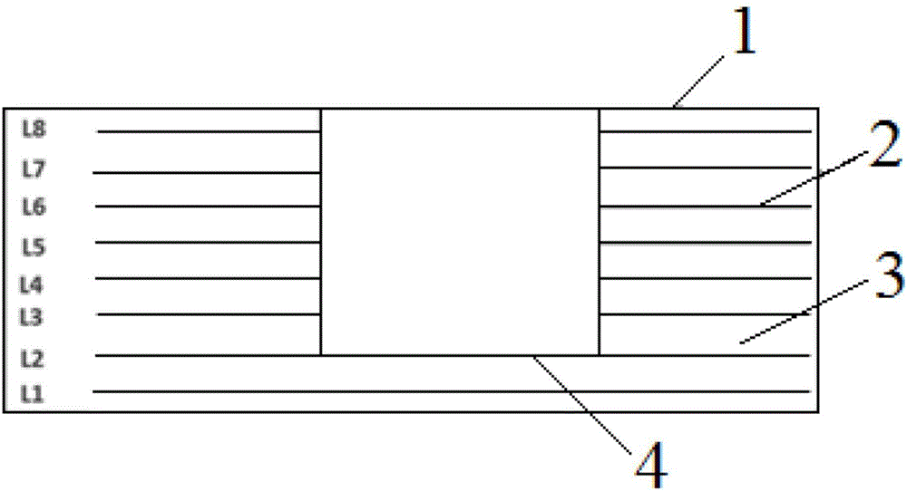
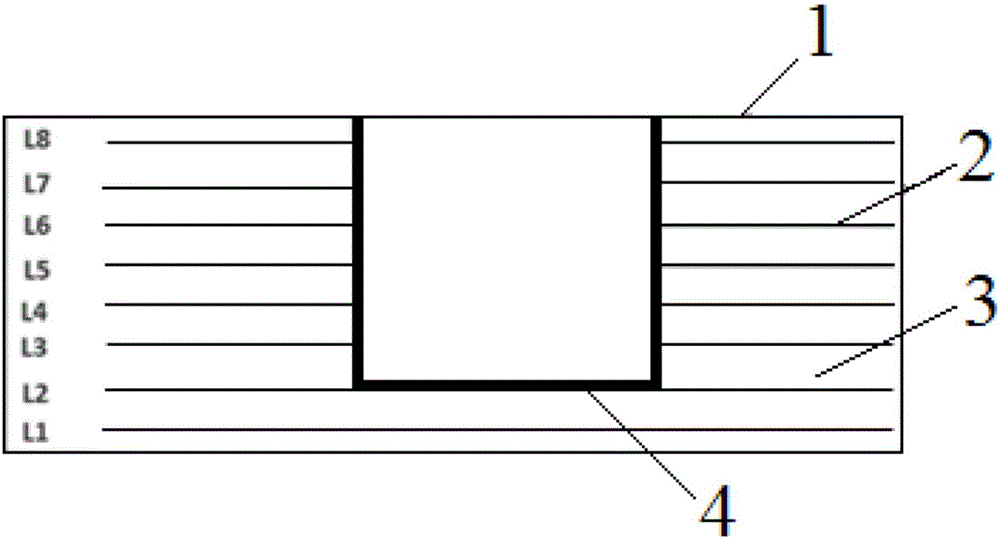
[0023] This embodiment provides a zero-tolerance controlled deep drilling method for a circuit board, which includes the following steps:

[0024] a. Cutting, cutting copper plates and prepregs and other incoming materials into plates of moderate size according to the design requirements of different plate sizes, removing the oily substance oxide film on the copper plate surface by conventional methods, and performing chemical microetching to make the copper surface occur Redox reaction roughens the copper surface.

[0025] b. Inner layer circuit pattern production, film production, after the required circuit pattern is made on the film film, the dry film is laminated on the surface of the inner core board, and the photosensitive film in the dry film is reacted by exposure, selective partial bridge After hardening, the dry film of the unexposed part is removed, and the photosensitive part is retained, thereby transferring the pattern on the film to the surface of the inner core pla...


PUM


Abstract

The invention discloses a zero-tolerance depth-controllable drilling method for a circuit board. The drilling method comprises a depth-controllable drilling process and a laser drilling process; in the depth-controllable drilling process, the drilling depth is 0-0.1 mm away from a target layer; and, in the laser drilling process, a medium layer on the surface of the target layer is removed, so that a zero-tolerance drilled hole is obtained. Because the mechanical depth-controllable drilling precision is 0.05 mm, the drilling depth is set to 0.05-0.1 mm away from the target layer when mechanical depth-controllable drilling is carried out; the problem that the distance between the mechanical drilling bottom and a next circuit layer is too small due to too-deep mechanical drilling or the next circuit layer of the target layer is drilled can be avoided; then, on the basis of mechanical depth-controllable drilling, laser drilling is carried out; after the medium layer on the surface of the target layer is removed; the hole depth achieves the target layer rightly; therefore, zero-tolerance depth-controllable drilling is realized; signal loss of micro-wave and radio-frequency products can be effectively reduced; the quality and the reliability of the circuit board are ensured; and requirements of clients on high-order products can be satisfied.

Description

Technical field [0001] The invention belongs to the technical field of printed circuit board manufacturing, and relates to a drilling method, in particular to a zero tolerance controlled deep drilling method for a circuit board. Background technique [0002] With the increasing requirements for PCBs (printed circuit boards, also known as printed circuit boards), and with the development of high-density assembly, in order to comply with the trend of miniaturization of circuit boards, high-density multilayer wiring has gradually become printed The development trend of circuit boards, in order to improve the wiring density, traditional printed circuit boards generally use plated through holes that penetrate the entire board thickness to achieve the purpose of three-dimensional connection. However, plated through holes often affect the freedom of wiring. For this problem, conductive blind holes or buried holes are generally used as a local three-dimensional connection method. For bli...

Claims


Application Information

Patent Timeline
Patent Type & Authority Applications(China)
IPC IPC(8): H05K3/42
CPCH05K3/42H05K2203/0214H05K2203/107
Inventor 周文涛宋清赵波喻恩
Owner SHENZHEN SUNTAK MULTILAYER PCB
Why Eureka
Try Eureka