
Screening method for improving yield of embedded flash memory

A screening method and embedded technology, applied in the wafer testing of embedded flash memory and the field of memory, can solve problems such as weak erasing ability, and achieve the effect of improving yield and reducing finished products.

Active Publication Date: 2017-02-22
SHANGHAI HUAHONG GRACE SEMICON MFG CORP
View PDF6 Cites 0 Cited by
  • Summary
  • Abstract
  • Description
  • Claims
  • Application Information

AI Technical Summary

Problems solved by technology

[0006] Many embedded flash memory products now require more and more storage capacity, which brings new challenges to the area control of the process memory unit and the logic circuit design of the chip design.
At the same time, there are different needs for product quality assurance. For burn-in testing, it is generally necessary to screen memory cells with weak erasability through weak current short-term erasure methods, which has a great impact on the control of process yield. Big challenge, so I hope to find a simpler and more concise way to deal with the process control problem of embedded flash memory

Method used


Image

  • Screening method for improving yield of embedded flash memory
  • Screening method for improving yield of embedded flash memory

Examples


Embodiment Construction

[0027] In order to make the content of the present invention clearer and easier to understand, the content of the present invention will be described in detail below in conjunction with specific embodiments and accompanying drawings.

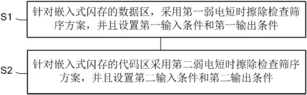
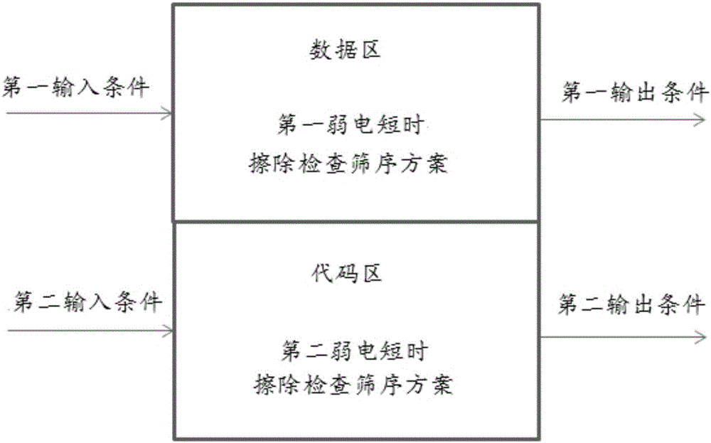
[0028] In the prior art, the adopted solution is to make the chip be repaired by more patches, so that the occupied area is relatively small; and in the prior art, for the data area and the code area defined differently from the customer, different areas provide the same A weak current short-term erasure inspection screening scheme.

[0029] In the prior art, if a single storage unit fails too much and the chip repair sector is not enough, it will be directly discarded; but this will cause a lot of waste. The present invention proposes to differentiate the quality of the bad storage sectors of the chip from the perspective of making the best use of everything, so as to make the treasure as useless as possible.

[0030] In the present invention,...


PUM


Abstract

The invention provides a screening method for improving the yield of an embedded flash memory. The method includes: a scheme using first weak currents to erase test sieve scale in a short-term manner is used for the data area of the embedded flash memory, and a scheme using second weak currents to erase test sieve scale in a short-term manner is used for the code area of the embedded flash memory, wherein the scheme using the first weak currents is different from the scheme using the second weak currents. In the prior art, input voltage and time are consistent, and output reading judging conditions are consistent. The method has the advantages that a design concept for adding a patch sector can be rejected, and the size of a chip can be controlled effectively; the yield can be increased as much as possible, materials are put into good use, and different market requirements are satisfied, the method is favorably applicable to the wafer test of the embedded flash memory, cost can be lowered for terminal customers, and productivity and efficiency are increased.

Description

technical field [0001] The present invention relates to the field of memory, in particular to the field of wafer testing of embedded flash memory; more specifically, the present invention relates to a screening method for improving the yield of embedded flash memory. Background technique [0002] Flash memory has become a research hotspot in non-volatile memory due to its convenience, high storage density, and good reliability. Since the first flash memory product came out in the 1980s, with the development of technology and the storage needs of various electronic products, flash memory has been widely used in mobile and communication devices such as mobile phones, notebooks, handheld computers and U disks. . [0003] Flash memory is a non-volatile memory. Its operating principle is to control the switch of the gate channel by changing the critical voltage of the transistor or memory cell to achieve the purpose of storing data, so that the data stored in the memory will not...

Claims


Application Information

Patent Timeline
IPC IPC(8): G11C29/04G11C29/00G11C29/56
CPCG11C29/006G11C29/04G11C29/56016G11C2029/0401G11C2029/0403
Inventor 任栋梁钱亮
Owner SHANGHAI HUAHONG GRACE SEMICON MFG CORP
Features
  • Generate Ideas
  • Intellectual Property
  • Life Sciences
  • Materials
  • Tech Scout
  • Unparalleled Data Quality
  • Higher Quality Content
  • 60% Fewer Hallucinations
Learn More