A LED microdisplay pixel unit structure for heterogeneous monolithic integration of Gan-based LEDs and TFTs
A technology of LED structure and monolithic integration, which is applied in the direction of electrical components, semiconductor devices, circuits, etc., can solve the problems of increasing pixel crosstalk and reducing display quality, and achieve the effect of improving stability, reliability and performance
Active Publication Date: 2019-07-05
SUN YAT SEN UNIV
View PDF3 Cites 0 Cited by
- Summary
- Abstract
- Description
- Claims
- Application Information
AI Technical Summary
Problems solved by technology
[0003] LED display is divided into two categories: passive addressing structure and active addressing structure. Passive addressing is more suitable for small area display. When the display area increases, the driving voltage increases and the crosstalk between pixels increases. , lowering the display quality
Method used
View moreImage
Smart ImageViewing Examples
Examples
Embodiment Construction
[0027] The drawings are for illustrative purposes only, and should not be construed as limitations on this patent; in order to better illustrate this embodiment, some parts in the drawings will be omitted, enlarged or reduced, and do not represent the size of the actual product;
[0028] For those skilled in the art, it is understandable that some well-known structures and descriptions thereof may be omitted in the drawings. The technical solutions of the present invention will be further described below in conjunction with the accompanying drawings and embodiments.
Login to View More PUM
 Abstract
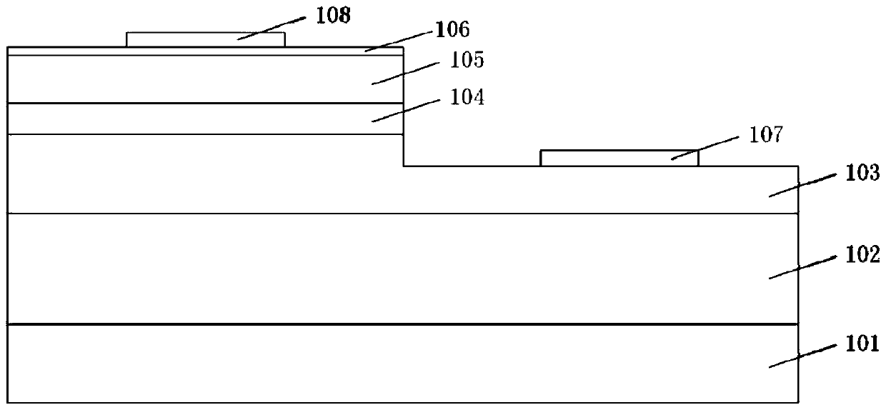
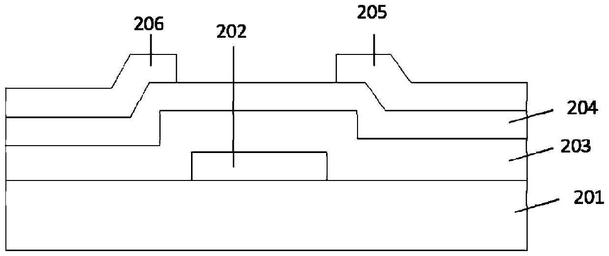
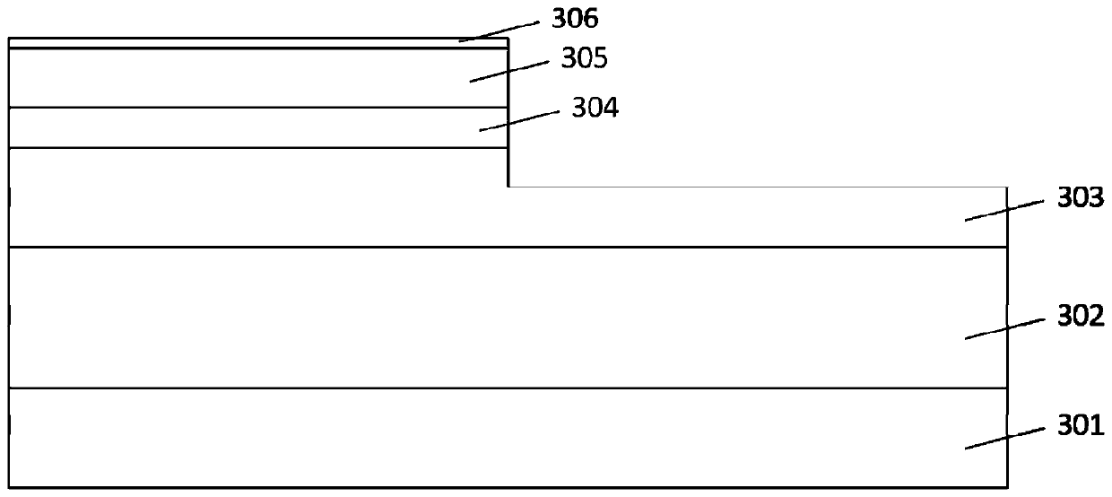
The invention provides an LED microdisplay pixel unit structure with heterogeneous monolithic integration of TFT and GaN-based LED. The structures comprises the two parts of a GaN-based LED structure and a TFT structure, wherein a u-GaN buffer layer, an n-GaN layer, an InGaN / GaN quantum well active layer, a p-GaN layer and an InGaN-based contact layer conduct epitaxy growth on a sapphire substrate of the GaN-based LED in sequence; the TFT structure conducts growth on an already produced LED chip modular construction and conducts growth of insulating layer, a TFT source electrode (also a P electrode of the LED), a TFT drain electrode, a semiconductor layer used as a TFT active layer, a gate insulation layer and a gate in sequence. According to the LED microdisplay pixel unit structure with the heterogeneous monolithic integration of the TFT and GaN-based LED, LED and TFT are integrated into one substrate, thus heterogeneous monolithic integration is achieved so that LED gray scale can be directly modulated, and electrical stability and integration level of the LED microdisplay is improved.
Description
technical field [0001] The invention relates to the field of semiconductor manufacturing technology and display, in particular to an LED micro-display pixel unit structure of GaN-based LED and TFT heterogeneous monolithic integration. Background technique [0002] LED has low power consumption, high luminous brightness, low radiation to the human body, long life, and can work in extreme environments. It is an energy-saving and environmentally friendly material. According to the three primary colors of red, green and blue, the LED light source can be combined with different light colors to realize image display. As a micro-array device, LED also has the characteristics of short response time and high modulation bandwidth, and has broad application prospects in the fields of micro-display and communication. [0003] LED display is divided into two categories: passive addressing structure and active addressing structure. Passive addressing is more suitable for small area displ...
Claims
Login to View More Application Information
Patent Timeline
 Patent Type & Authority Patents(China)
IPC IPC(8): H01L27/12
CPCH01L27/1214
Inventor 刘立林张向英
Owner SUN YAT SEN UNIV


