Supercharge Your Innovation With Domain-Expert AI Agents!

Non-volatile storage memory module with physical-to-physical address remapping

A memory module, non-volatile technology used in the field of memory systems to solve problems such as reducing consumer lifespan

Active Publication Date: 2017-02-22
SANDISK TECH LLC
View PDF6 Cites 3 Cited by
  • Summary
  • Abstract
  • Description
  • Claims
  • Application Information

AI Technical Summary

Problems solved by technology

Certain tests performed in traditional manufacturing workflows require a large number of P / E cycles on the flash memory, reducing the possible remaining life of the consumer

Method used


Image

  • Non-volatile storage memory module with physical-to-physical address remapping
  • Non-volatile storage memory module with physical-to-physical address remapping
  • Non-volatile storage memory module with physical-to-physical address remapping

Examples


Embodiment Construction

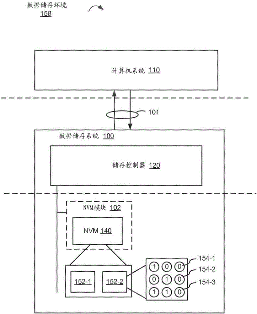
[0017] Regardless of what type of memory element (e.g., individual memory cells in a memory die) is used in a storage system, or how such memory elements are configured (e.g., 2D configuration, 3D configuration), memory elements are sometimes cause failure. The manufacturing process for such memory elements has a certain yield, meaning that some as-manufactured memory elements may be "bad" from the start. Other memory elements are severely damaged after fabrication. In conventional processing, memory dies are integrated before being incorporated into a larger memory device (e.g., memory module 102, Figure 1A ), perform extensive testing to convert the memory die (e.g., NVM die 140, Figure 1A ) into different classes (eg, based on the operating portion or function of the memory elements in such a memory die). For example, severely damaged fabricated memory elements typically often fail the so-called "burn-in" test, rendering portions of the memory die (eg, pages, blocks, die...


PUM


Abstract

The various embodiments described herein include systems, methods and / or devices used to enable physical-to-physical address remapping in a storage module. In one aspect, the method includes, for each of a sequence of two or more units of non-volatile memory, determining a validity state of a respective unit of memory. In accordance with a determination that the validity state of the respective unit of memory is an invalid state, the method includes storing, in a table, a second address assigned to the respective unit of memory. At least a portion of the second address is a physical address portion corresponding to a physical location of a second unit of memory. In accordance with a determination that the validity state of the respective unit of memory is a valid state, the method includes forgoing assignment of the second address corresponding to the unit of memory.

Description

technical field [0001] The disclosed embodiments relate generally to memory systems, and in particular to physical-to-physical address remapping in memory devices. Background technique [0002] Semiconductor memory devices, including flash memory, typically utilize memory cells to store data as electrical values, such as charge or voltage. A flash memory cell, for example, includes a single transistor with a floating gate that is used to store an electrical charge representation of a data value. Flash memory is a non-volatile data storage device that can be electrically erased and reprogrammed. More generally, nonvolatile memory (e.g., flash memory, and other types of nonvolatile memory implemented using any of a variety of technologies) retains stored information even when power is not applied, as opposed to requiring power to maintain stored information. Volatile memory of information is the opposite. [0003] Traditional manufacturing workflows utilize extensive testin...

Claims


Application Information

Patent Timeline
IPC IPC(8): G11C29/00
CPCG11C29/765G11C29/785G06F12/0246G06F2212/1032G06F2212/7209G06F11/2094G06F12/0623G11C29/44
Inventor J.E.弗拉耶M.维德亚布胡尚
Owner SANDISK TECH LLC
Features
  • R&D
  • Intellectual Property
  • Life Sciences
  • Materials
  • Tech Scout
  • Unparalleled Data Quality
  • Higher Quality Content
  • 60% Fewer Hallucinations
Learn More