Three-dimensional on-chip network test planning method

A technology of test planning and network-on-chip, which is applied in software testing/debugging, error detection/correction, and special data processing applications, etc. It can solve problems such as insufficient optimization effect of test planning algorithms and limited application range of models, achieving short test time, The effect of low power consumption and increased diversity

Active Publication Date: 2017-03-15
GUILIN UNIV OF ELECTRONIC TECH
View PDF4 Cites 12 Cited by
  • Summary
  • Abstract
  • Description
  • Claims
  • Application Information

AI Technical Summary

Problems solved by technology

[0004] The technical problem to be solved by the present invention is that the scope of application of the model in the existing test planning research...

Method used


Image

  • Three-dimensional on-chip network test planning method
  • Three-dimensional on-chip network test planning method
  • Three-dimensional on-chip network test planning method

Examples


Embodiment Construction

[0041] The present invention will be described below in conjunction with the accompanying drawings and embodiments, but not to limit the content of the present invention.

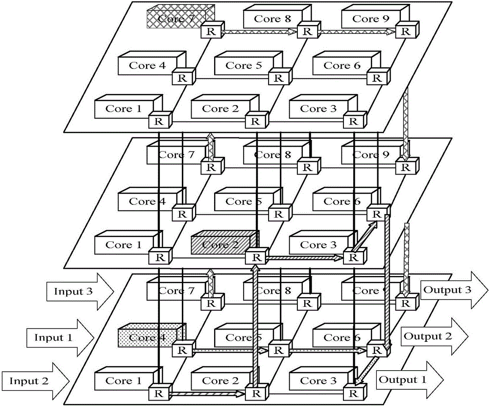
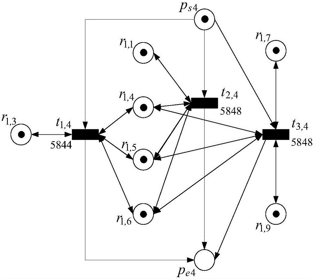
[0042] The 3D NoC involved in the preferred embodiment of the present invention is a 3D Mesh topology, such as figure 1 As shown, two-dimensional chips with multiple planar structures are vertically interconnected through silicon via technology, that is, they are mainly composed of IP cores, routing nodes, network interfaces, and communication links. The communication link includes interconnection lines in XY direction and TSV (Through Silicon Via) in Z direction. The routers in the 3D NoC adopt the wormhole data exchange mechanism based on the virtual channel technology, and the routing algorithm adopts the XYZ routing algorithm, and each router connects to the resource nodes through the resource network interface. Since 3D NoC supports high-efficiency and reusable design, it adopts distributed technology...


PUM


Abstract

The invention discloses a three-dimensional on-chip network test planning method. A time Petri network model is established in combination with the characteristics of 3D NoC testing, a change excitation sequence serves as a parallel test task planning scheme, sequential scheduling optimization is carried out based on test path allocation through an improved two-stage hierarchical bat algorithm, and test resources are reasonably and effectively allocated to various IP cores. The model visually describes the 3D NoC test planning problem, the 3D NoC test time can be effectively shortened, test efficiency can be improved, and test effectiveness can be guaranteed. The test planning algorithm has certain advantages on the aspects of the quality of solutions and the convergence rate, the efficiency of parallel testing can be effectively improved, and the test time can be shortened.

Description

technical field [0001] The present invention relates to the technical field of three-dimensional network-on-chip (3D NoC), in particular to a three-dimensional network-on-chip test planning method. Background technique [0002] With the substantial expansion of the scale of integrated circuits, the traditional network-on-chip is limited by the layout conditions of the planar structure, and the interconnection lines are long, which will increase the delay and power consumption of data transmission. The emergence of 3D IC technology has broken the limitation of the planar structure. This technology stacks two-dimensional NoC between layers through silicon vias, increasing the vertical expansion. 3D NoC, which combines 3D IC and NoC technology, has attracted the attention of researchers. The advantages of 3D NoC are mainly manifested in: 1. The vertical interconnection line shortens the length of the global interconnection line, has lower transmission power consumption and del...

Claims


Application Information

Patent Timeline
IPC IPC(8): G06F17/50G06F11/36
CPCG06F11/3684G06F30/22
Inventor 胡聪贾梦怡周甜万春霆许川佩朱望纯屈瑾瑾
Owner GUILIN UNIV OF ELECTRONIC TECH
Why Eureka
Try Eureka