

Ring part structure and machining method thereof
A processing method and ring technology, which is applied in the ring structure and its processing field, can solve the problems of spalling and tip discharge particles, and achieve the possible effects of reducing the tip, improving the service life, and reducing the phenomenon of peeling of attached particles
- Summary
- Abstract
- Description
- Claims
- Application Information
AI Technical Summary
Problems solved by technology
Method used
Image

Examples
Embodiment Construction
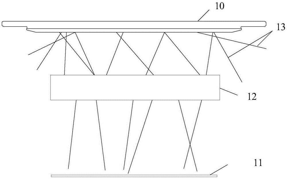
[0035] It can be seen from the background art that the rings in the prior art have the problem that the surface of the pattern is prone to tip discharge or peeling off of the adsorbed particles. Now combine the structure of the ring to analyze the causes of the tip discharge and the peeling off of the adsorbed particles:
[0036] As mentioned in the background technology, the ring has two main functions in the sputtering process: one is to restrict the trajectory of the sputtered ions and play a role of focusing; the other is to absorb the particles produced in the sputtering process to purify role.
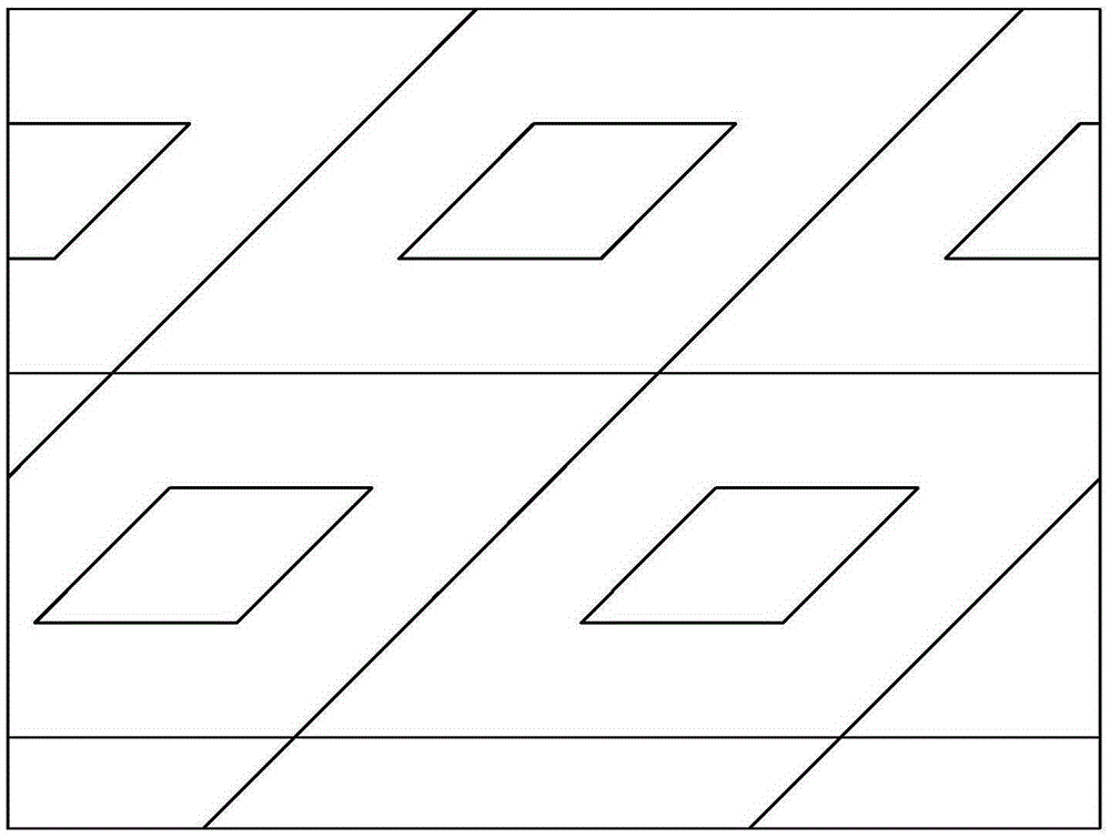
[0037] refer to figure 2 ,show figure 1 Schematic diagram of the pattern on the surface of the middle ring.
[0038] In order to improve the adsorption capacity of the ring to particles, the surface of the ring is provided with patterns to increase the roughness of the surface of the ring and improve the adsorption capacity of the surface of the ring. However, if the pattern...
PUM
 Abstract
Description
Claims
Application Information