Wafer level dynamic pre-burning test method

A test method and wafer-level technology, applied in the field of testing, can solve the problems of large packaging and testing costs, expenses, and inability to effectively reduce production costs, and achieve the effect of reducing packaging and testing costs

Active Publication Date: 2017-03-22
POWERCHIP SEMICON MFG CORP
View PDF5 Cites 0 Cited by
  • Summary
  • Abstract
  • Description
  • Claims
  • Application Information

AI Technical Summary

Problems solved by technology

[0003] Generally, the burn-in test is performed after the memory has been assembled or packaged. Therefore, if the detected components are defective, they cannot be repaired or re-assembled by laser. Such a test method requires Spend considerable packaging and testing costs, resulting in reduced production capacity
[0004] In order to further reduce production costs, some people have proposed to perform related defect detection before packaging, such as Wafer Level Burn-In (WLBI) test, so that the reliability of the product can be verified during the wafer test stage, and then Since some tests still have to be performed after packaging, such as the dynamic operation burn-in test, it cannot really effectively reduce the production cost, that is, the burn-in test in the prior art still has improvements Space

Method used


Image

  • Wafer level dynamic pre-burning test method
  • Wafer level dynamic pre-burning test method
  • Wafer level dynamic pre-burning test method

Examples


Embodiment Construction

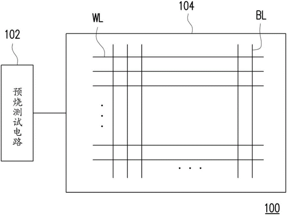
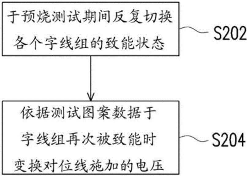
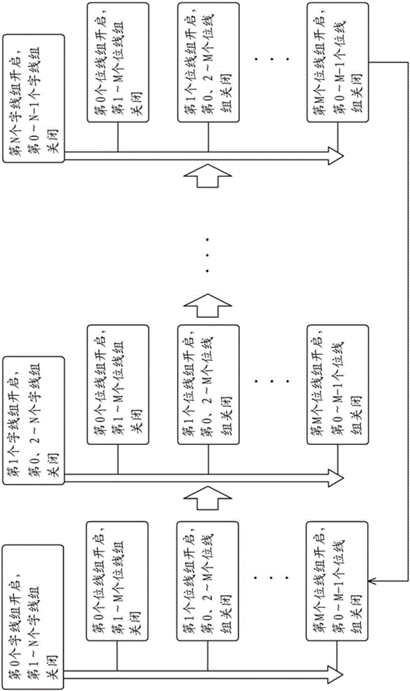
[0021] figure 1 is a schematic diagram of a memory chip of a wafer according to an embodiment of the present invention, figure 2 is a schematic flow chart of a wafer-level dynamic burn-in test method according to an embodiment of the present invention, please refer to figure 1 and figure 2 . A wafer (not shown) may include multiple memory chips. For ease of illustration, only one memory chip 100 is shown in this embodiment for illustration. In fact, the memory chips in the wafer can be burn-in tested at the same time. The memory chip 100 may include a burn-in test circuit 102 and a memory array 104, wherein the memory array 104 includes a plurality of word lines WL and a plurality of bit lines BL, and the intersection of the word lines WL and the bit lines BL is configured with the word line WL and the bit lines BL-connected memory cells (not shown). The word line WL can be divided into multiple word line groups, and the burn-in test circuit 102 can receive a burn-in tes...


PUM


Abstract

A wafer level dynamic pre-burning test method is provided. The energization state of each word line group is repeatedly switched during the pre-firing test and the voltage applied to the bit line is converted according to the test pattern data when the word line group is again energized.

Description

technical field [0001] The invention relates to a test method, in particular to a wafer-level dynamic burn-in test method. Background technique [0002] With the vigorous development of semiconductor technology, the volume of electronic components is also becoming lighter, thinner, shorter and smaller. After the electronic components are manufactured, the electronic components usually undergo a burn-in test first, so as to test the electronic components with a short life cycle in an environment of high temperature, high voltage and high current. In this way, the reliability of the product can be improved. [0003] Generally, the burn-in test is performed after the memory has been assembled or packaged. Therefore, if the detected components are defective, they cannot be repaired or re-assembled by laser. Such a test method requires It costs a lot of packaging and testing costs, which reduces the production capacity. [0004] In order to further reduce production costs, som...

Claims


Application Information

Patent Timeline
IPC IPC(8): G11C29/56
Inventor 黄贤纬苏圣峰刘东昱李瀛洲
Owner POWERCHIP SEMICON MFG CORP
Why Eureka
Try Eureka