
Chip comprising eFuse module, electronic device and chip burning control method

A chip, read control technology, applied in electrical digital data processing, architecture with a single central processing unit, instruments, etc., can solve the problem of too many chip pins, and achieve the effect of reducing the cost of packaging and testing

Pending Publication Date: 2022-04-22
厦门码灵半导体技术有限公司
View PDF0 Cites 0 Cited by
  • Summary
  • Abstract
  • Description
  • Claims
  • Application Information

AI Technical Summary

Problems solved by technology

[0003] In order to solve the existing technical problem of too many chip pins including the eFuse module, the present invention provides a chip including the eFuse module, an electronic device and a chip programming control method, which can reduce the pins of the chip while ensuring the security of the chip information. Reduce chip packaging and testing costs

Method used


Image

  • Chip comprising eFuse module, electronic device and chip burning control method
  • Chip comprising eFuse module, electronic device and chip burning control method
  • Chip comprising eFuse module, electronic device and chip burning control method

Examples


Embodiment

[0068] In order to solve the existing technical problem of too many chip pins including the eFuse module, the present invention provides a chip including the eFuse module, an electronic device and a chip burning control method, which can reduce the pins of the chip while ensuring the security of the chip information. Reduce chip packaging and testing costs.

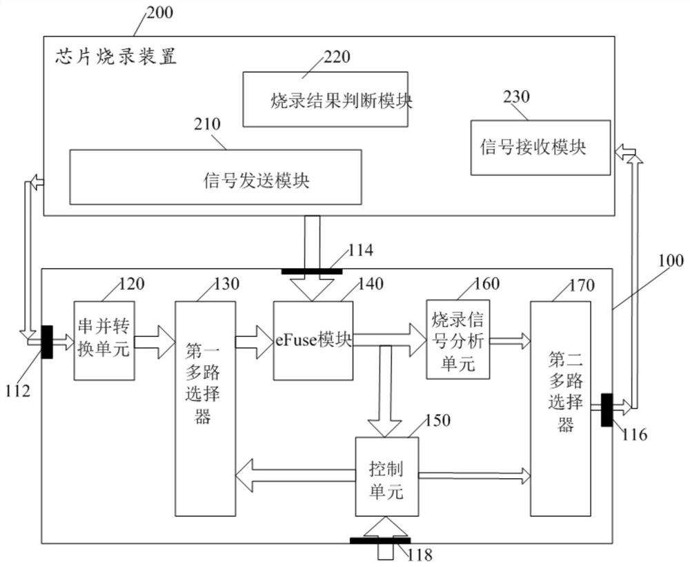
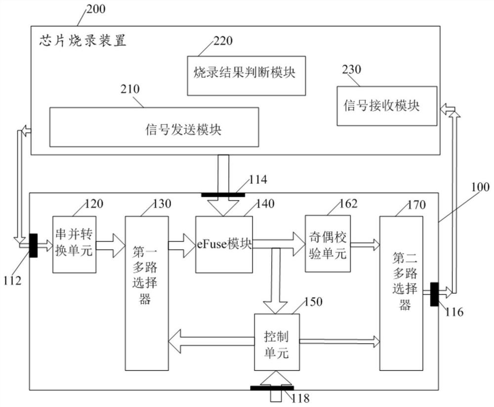
[0069] Such as figure 2 As shown, the present embodiment provides a chip including an eFuse module, and the chip 100 includes:

[0070] eFuse module 140, serial-to-parallel conversion unit 120, programming signal analysis unit 160, control unit 150 and pins,

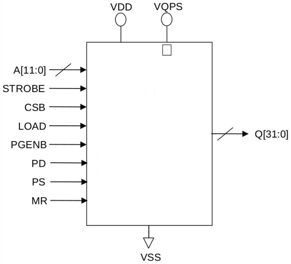
[0071] The pins include a serial input signal pin 112, programming and reading control signal pins 114, 118 and an output signal pin 116; pin 114 is a necessary control signal for eFuse programming, such as Figure 1 As shown (control signals such as STROBE, CSB, LOAD, PGENB, PD, etc.), pin 118 is the reset and clock signal necessary for the work in the SoC, main...


PUM


Abstract

The invention belongs to the technical field of integrated circuits, and provides a chip comprising an eFuse module, an electronic device and a chip burning control method in order to solve the technical problem that an existing chip comprising the eFuse module is too many in pin, and the chip comprises the eFuse module, a serial-parallel conversion unit, a burning signal analysis unit, a control unit and pins. The pins comprise a serial input signal pin, a burning reading control signal pin and an output signal pin, and the serial-parallel conversion unit is used for converting a serial input signal input through the serial input signal pin into a parallel input address signal; the eFuse module is used for burning corresponding bits of the parallel input address signals converted by the serial-parallel conversion unit; and the burning signal analysis unit is used for generating a corresponding burning state signal based on the burning signal processed by the eFuse module, and the burning state signal is output through the output signal pin. Therefore, the number of pins of the chip is reduced while the information security of the chip is ensured, and the packaging and testing cost of the chip is reduced.

Description

technical field [0001] The invention relates to the technical field of integrated circuits, in particular to a chip including an eFuse module, an electronic device and a chip programming control method. Background technique [0002] At present, the security encryption function of control units such as MCU, MPU, and CPU of various architectures is generally realized by the built-in eFuse module. The built-in eFuse module can be used to load chip ID, chip production package, key and other information. Such information sometimes needs to be written by the manufacturer in the CP and FT links, and some needs to be written by the end user, so the pins related to eFuse programming must be drawn out in the package. At the same time, it is necessary to meet the requirements of the burned information that cannot be read by the non-burning party. With the continuous development and iteration of electronic product technology, customers have higher and higher safety requirements, and t...

Claims


Application Information

Patent Timeline
IPC IPC(8): G06F15/78
CPCG06F15/7817
Inventor 陈毓良张敏温建刚梁梦雷
Owner 厦门码灵半导体技术有限公司
Learn More