Semiconductor device and inspection method of the same and electromagnetic detection equipment

A technology for integrated circuits and detection devices, applied in measurement devices, semiconductor/solid-state device testing/measurement, semiconductor devices, etc., can solve the problems of inability to obtain chip information, and it takes more time to obtain chip information. ensure safe effect

Inactive Publication Date: 2006-08-30
PANASONIC CORP
View PDF2 Cites 4 Cited by
  • Summary
  • Abstract
  • Description
  • Claims
  • Application Information

AI Technical Summary

Problems solved by technology

[0008] However, it can be expected that semiconductor integrated circuits that emphasize fewer pins and safety will be expected in the future. As semiconductor devices become more complex, it is predicted that chip information cannot be obtained, or even if a scanning circuit can be installed, it is difficult to obtain chip information. Information takes more time etc.
In addition, since there is an output port to the outside, there is also a great danger from the viewpoint of safety.

Method used


Image

  • Semiconductor device and inspection method of the same and electromagnetic detection equipment
  • Semiconductor device and inspection method of the same and electromagnetic detection equipment
  • Semiconductor device and inspection method of the same and electromagnetic detection equipment

Examples


Embodiment Construction

[0068] Next, the semiconductor integrated circuit of the present invention will be described based on specific examples.

[0069] (Embodiment 1)

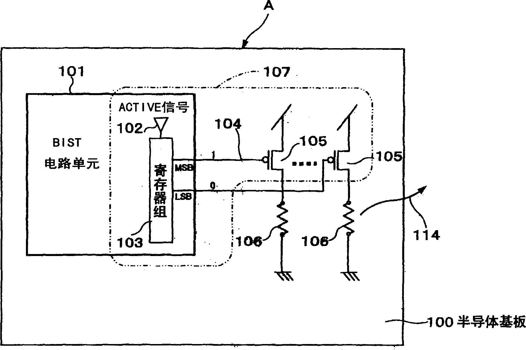
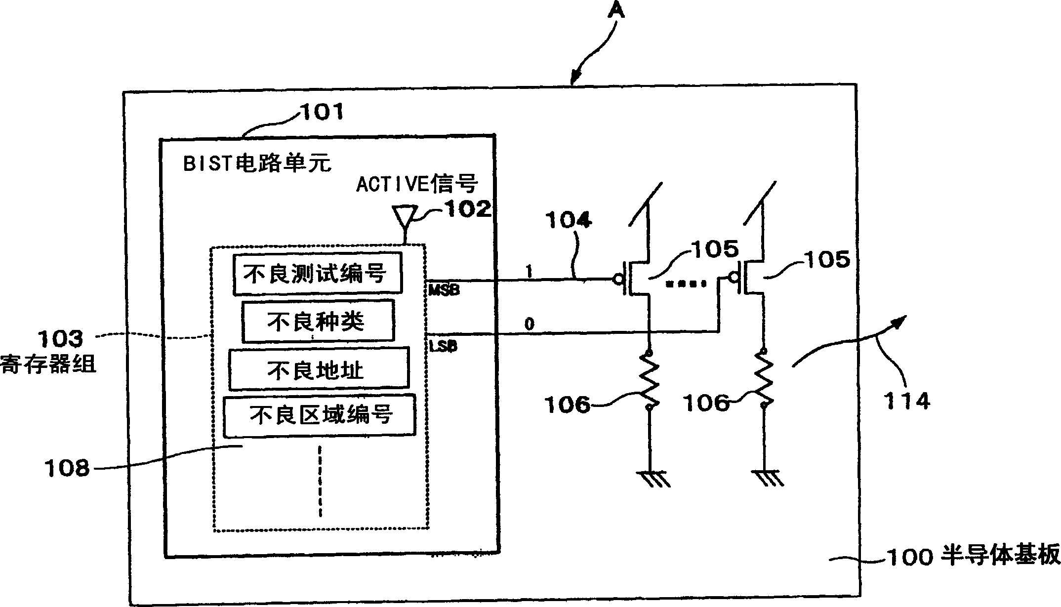
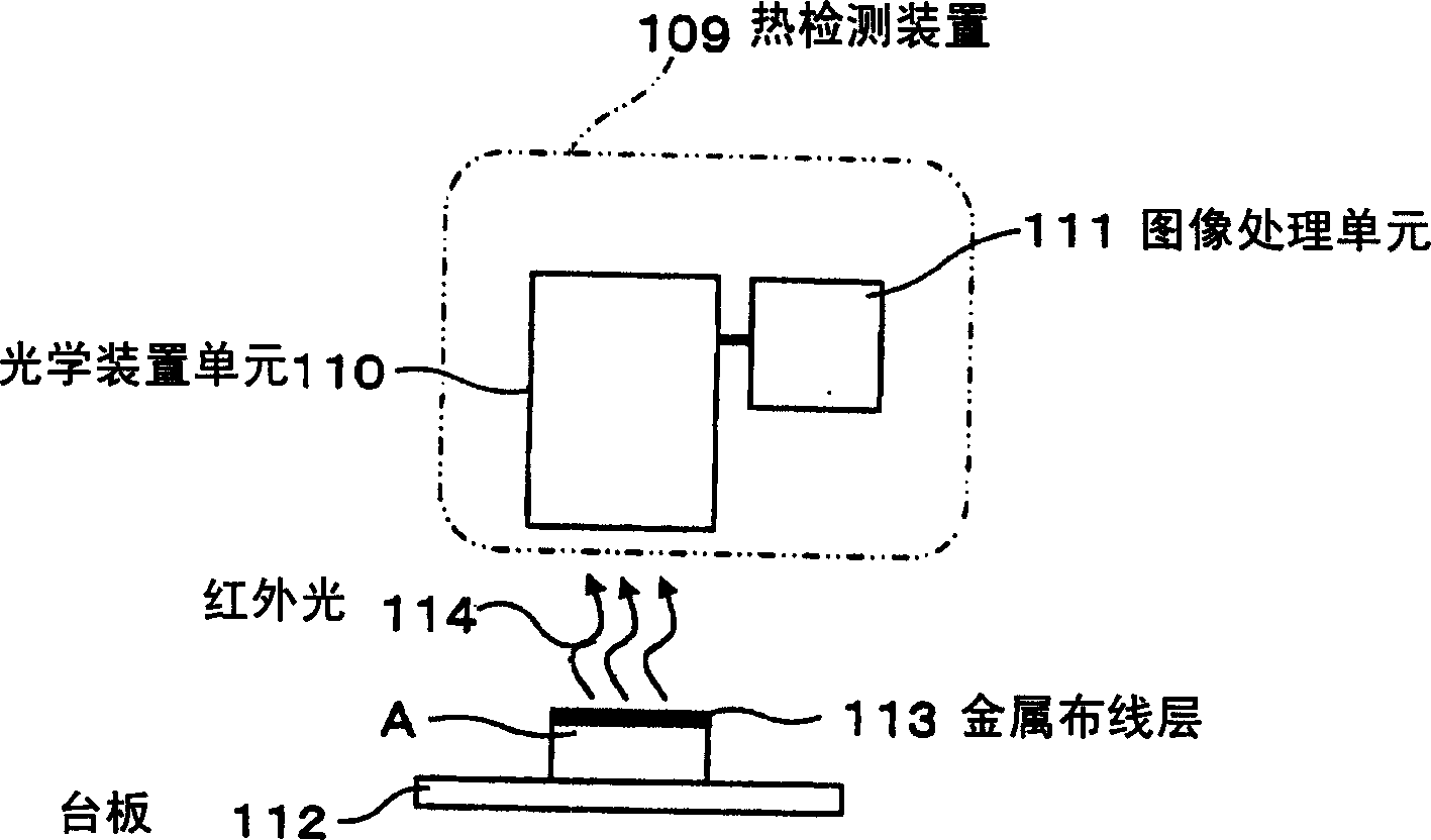
[0070] according to Figure 1 ~ Figure 3A and Figure 3B A semiconductor integrated circuit A having an element that outputs thermal energy, which is one type of electromagnetic waves, which outputs chip information, and a thermal detection device as an electromagnetic wave detection device for reading will be described.

[0071] like figure 1 As shown, on the semiconductor substrate 100 of the semiconductor integrated circuit A that constitutes the circuit for realizing the target function, a BIST (Built In Self Test, internal self-test) circuit unit 101, an element 105, and a BIST (Built In Self Test) circuit unit 101, an element 105, and Resistor 106 that causes heating. In addition, in this example, the register group 103 and the element 105 constitute a control circuit 107 for activating the semiconductor substrate with a p...


PUM


Abstract

A semiconductor integrated circuit and its inspection method, and an electromagnetic detection equipment, the semiconductor integrated circuit including, without setting an extra external test terminal, a control circuit for outputting chip information and resistors driven for generating thermal energy that is a kind of electromagnetic waves to obtain manufacturing information and inspection information in a contactless manner, so that a system thus configured operate in synchronization with an automated test equipment (ATM). Consequently, in an actual semiconductor integrated circuit, it is possible to improve quality while achieving security.

Description

technical field [0001] The present invention relates to the ease of inspection of semiconductor integrated circuits emphasizing fewer pins and safety. Background technique [0002] In a semiconductor integrated circuit where the safety of fewer pins is emphasized due to restrictions on the number of pins, chip size, and safety, it is difficult to install a test circuit, resulting in a situation where it is difficult to obtain information that can be inspected every year. [0003] In the conventional inspection method, in order to confirm the degree of completion of the semiconductor integrated circuit at the actual product level, a separately designed means to obtain inspection information using the semiconductor integrated circuit before the product, or a dedicated test input and output terminal, and a test dedicated mode, Generally, it is a means of checking information such as serially outputting test results represented by boundary scan testing. [0004] In addition, in...

Claims


Application Information

Patent Timeline
Patent Type & Authority Applications(China)
IPC IPC(8): H01L27/02H01L21/66G01R31/00
CPCG11C29/48G11C29/44G11C2029/4402G11C29/1201
Inventor 三嶌智史
Owner PANASONIC CORP
Why Eureka
Try Eureka