Supercharge Your Innovation With Domain-Expert AI Agents!

Turn-off power semiconductor device with improved centering and fixing of gate ring, and method for manufacturing same

一种功率半导体、半导体的技术,应用在半导体/固态器件制造、半导体器件、半导体/固态器件零部件等方向,能够解决晶片破裂、电气故障、橡胶环损坏等问题

Active Publication Date: 2017-03-22
HITACHI ENERGY LTD
View PDF6 Cites 2 Cited by
  • Summary
  • Abstract
  • Description
  • Claims
  • Application Information

AI Technical Summary

Problems solved by technology

This can cause cracking of the wafer, damage to the rubber ring or electrical failure (non-homogeneous contact between grid ring and ring grid contact)

Method used


Image

  • Turn-off power semiconductor device with improved centering and fixing of gate ring, and method for manufacturing same
  • Turn-off power semiconductor device with improved centering and fixing of gate ring, and method for manufacturing same
  • Turn-off power semiconductor device with improved centering and fixing of gate ring, and method for manufacturing same

Examples


Embodiment Construction

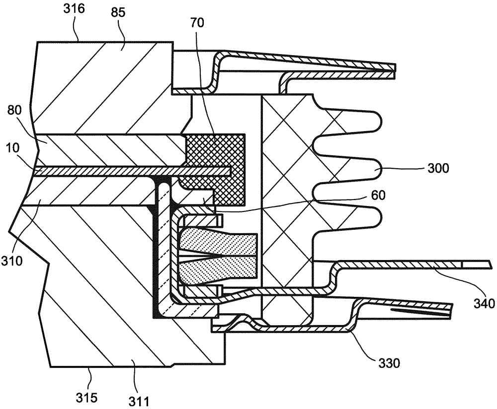
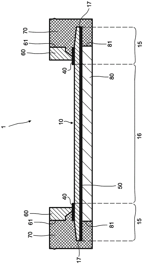
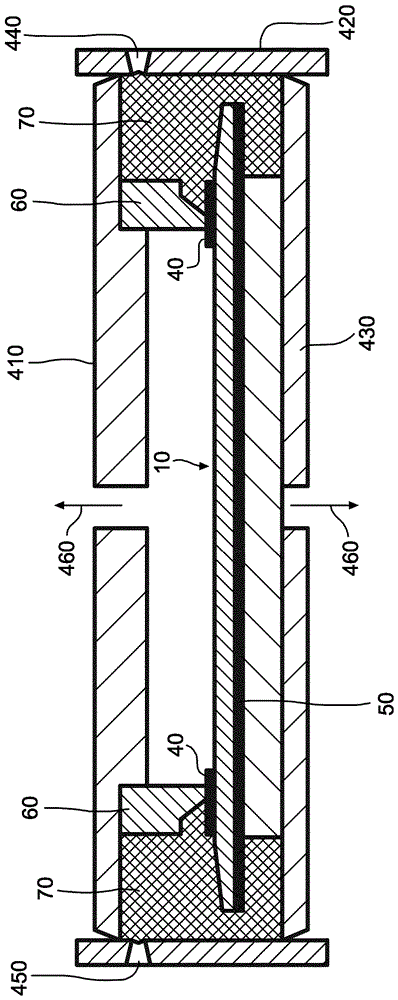
[0036] figure 1 The turn-off power semiconductor device according to the first embodiment of the invention shown in cross section is a reverse conducting integrated gate commutated thyristor (RC-IGCT) 1 comprising a wafer 10 , a conductive gate ring 60 and a rubber ring 70 . as in Figure 2A (which shows along the Figure 2BAs can best be seen in the cross-section of the wafer 10 in line AA' in ), the wafer 10 has a first main side 11 and a second main side 12, which are parallel to the first main side 11 and extend laterally. The wafer comprises an active region 16 (inner region) and a termination region (edge ​​region) 15 surrounding the active region 16 . In the active region 16 of the wafer 10 a plurality of thyristor cells 2 and a single freewheeling diode 3 are provided between the first main side 11 and the second main side 12 .

[0037] Each thyristor cell 2 comprises, from the first main side 11 to the second main side 12 of the wafer 10, a first cathode electrode ...


PUM


Abstract

The present invention relates to a turn-off power semiconductor device (1) having a wafer (10) with an active region and a termination region surrounding the active region, a rubber ring (70) as an edge passivation for the wafer (10) and a gate ring (60) placed on a ring-shaped gate contact (40) on the termination region for contacting the gate electrodes of at least one thyristor cell formed in the active region of the wafer. In the turn-off power semiconductor device (1) of the invention, the outer circumferential surface of the gate ring is in contact with the rubber ring to define the inner border of the rubber ring (70). In the invention the area consumed by the ring-shaped gate contact (40) on the termination or edge region can be minimized. The upper surface of the gate ring (60) and the upper surface of the rubber ring (70) form a continuous surface extending in a plane parallel to the first main side (11) of the wafer (10). In a method for manufacturing the device, the gate ring (60) is used as an inner sidewall of a mold for molding the rubber ring (70).

Description

technical field [0001] The invention relates to a turn-off power semiconductor arrangement as stated in the preamble of claim 1 and to a method for producing such a turn-off power semiconductor arrangement. Background technique [0002] A gate turn-off thyristor (GTO) is known from US 2009 / 096503 A1, in which the gate electrode of the substrate is contacted by a ring-shaped contact element. A ring-shaped passivation member is disposed at the edge of the semiconductor substrate surrounding the ring-shaped gate contact element. [0003] From JP 07-312420 A a gate turn-off thyristor (GTO) is known in which a needle-shaped ring frame electrode is soldered on the surface of the gate electrode of the semiconductor device. The insulating coating material covers the edges of the semiconductor device. [0004] From US 4370180 A a gate turn-off thyristor (GTO) is known, in which the periphery of the substrate is encapsulated by silicone rubber for passivation. [0005] Known prior ...

Claims


Application Information

Patent Timeline
Patent Type & Authority Applications(China)
IPC IPC(8): H01L23/051H01L23/31
CPCH01L23/051H01L23/3185H01L2924/0002H01L2924/00H01L29/7416H01L29/744H01L2924/1302H01L2924/13055H01L21/565H01L29/45H01L29/66363H01L29/7424H01L29/745
Inventor H.拉韦纳T.维克斯特伦H.阿姆斯图茨N.迈尔
Owner HITACHI ENERGY LTD
Features
  • R&D
  • Intellectual Property
  • Life Sciences
  • Materials
  • Tech Scout
  • Unparalleled Data Quality
  • Higher Quality Content
  • 60% Fewer Hallucinations
Learn More