Semiconductor device

A semiconductor and conductor layer technology, applied in semiconductor devices, electrical components, circuits, etc., can solve problems such as strong effect, and achieve the effect of suppressing the drop of withstand voltage

Active Publication Date: 2020-08-07
SANKEN ELECTRIC CO LTD
View PDF5 Cites 0 Cited by
  • Summary
  • Abstract
  • Description
  • Claims
  • Application Information

AI Technical Summary

Problems solved by technology

If the thickness of the insulating film provided between the n-region surface outside the RESURF region and the conductor film constituting the capacitive FP is the same as the thickness of the insulating film between the conductor film constituting the capacitive FP on the RESURF region and the substrate surface, Then there is the following problem: the potential division effect caused by the capacitive FP on the surface of the n-region outside the RESURF region is strong, and the depletion layer is easy to reach the end of the n-region.

Method used


Image

  • Semiconductor device
  • Semiconductor device
  • Semiconductor device

Examples


Embodiment Construction

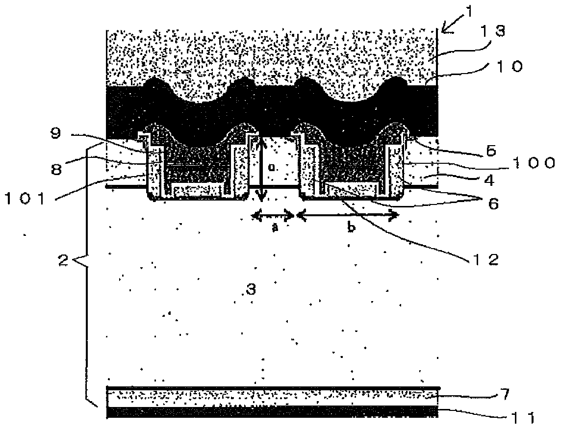
[0016] Next, a semiconductor device 1 as an embodiment of the present invention will be described.

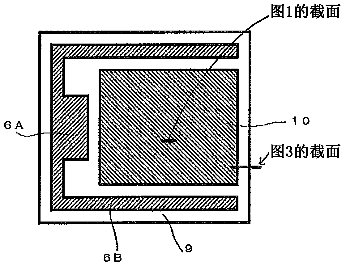
[0017] figure 1 A cross-sectional view of the semiconductor device 1 is shown. This semiconductor device 1 includes a trench gate type element portion (active region) formed on a semiconductor base 2 made of silicon. In this semiconductor substrate 2, an n-layer (first semiconductor region) 3 serving as a drift region and a p- layer (second semiconductor region) 4 serving as a base region are sequentially formed on a p-layer 7 serving as a collector region. Grooves (gate trenches) 100 are formed on the surface side of the semiconductor substrate 2 , and the grooves 100 penetrate the p − layer 4 and reach the n − layer 3 at the bottom. Slot 100 in with figure 1 Extended in the vertical direction of the paper, although not in the figure 2 shown in the top view, but in the figure 2 A plurality of parallel grooves 100 are formed in the longitudinal direction of the paper. I...


PUM


Abstract

A semiconductor device. It aims to solve the following problems: the potential division effect of the capacitive FP is strong, and the depletion layer can easily reach the end of the n-region. It is characterized in that the edge region has: a semiconductor base; a semiconductor region of a second conductivity type opposite to the first conductivity type, which is arranged in the semiconductor base in a pn-bonded manner; and a conductor layer above and on the semiconductor region. A plurality of the conductor layers are arranged side by side above the region outside the semiconductor region, the conductor layer is insulated from the semiconductor region and the region outside the semiconductor region, and the conductor layer above the region outside the semiconductor region is separated from the upper surface of the region outside the semiconductor region The distance between them is greater than the distance between the conductor layer above the semiconductor region and the upper surface of the conductor region. The distance between the conductor layer above the semiconductor base and the upper surface of the semiconductor base is greater than the distance between the conductor layer above the semiconductor region and the upper surface of the semiconductor region.

Description

technical field [0001] The present invention relates to a semiconductor device having a fringe region with improved withstand voltage outside an active region. Background technique [0002] 11 of Patent Document 1 discloses the structure of a semiconductor device provided with a RESURF (Reduced Surface Field) region composed of a second conductivity type opposite to the first conductivity type, and performing pn combination with the semiconductor substrate of the first conductivity type; and a capacitive field electrode, which is arranged above the RESURF region. [0003] For example, there is an impurity concentration (1×10 15 ~1×10 17 [ / cm 3 ]) The specific impurity concentration is 1×10 17 ~1×10 18 [ / cm 3 ] The base area is a small RESURF area. The RESURF region further extends the depletion layer of the semiconductor substrate away from the active region, and can make the curvature of the depletion layer gentler. However, since the impurity concentration of the R...

Claims


Application Information

Patent Timeline
Patent Type & Authority Patents(China)
IPC IPC(8): H01L29/739H01L29/06
CPCH01L29/063H01L29/7397
Inventor 鸟居克行
Owner SANKEN ELECTRIC CO LTD
Why Eureka
Try Eureka