Chip package structure and method

A chip packaging structure and chip packaging technology, applied in the direction of electrical components, electric solid devices, circuits, etc., can solve the problems of unfavorable chip heat dissipation, large thickness, etc., and achieve the effect of increasing interconnect channel density, reducing restrictions, and increasing bandwidth

Inactive Publication Date: 2017-04-05
HUAWEI TECH CO LTD
View PDF6 Cites 34 Cited by
  • Summary
  • Abstract
  • Description
  • Claims
  • Application Information

AI Technical Summary

Problems solved by technology

[0004] However, encapsulating chips with two substrates makes the entire package structure (including: upper substrate, MC, target chip and lower substrate) thicker (for example, about 490 microns (μm)), which cannot meet the needs of semiconductor packaging in current technologies. The demand for smaller and thinner is also not conducive to the heat dissipation of the chip

Method used


Image

  • Chip package structure and method
  • Chip package structure and method
  • Chip package structure and method

Examples


Embodiment Construction

[0121] The technical solutions in the embodiments of the present application will be clearly described below with reference to the drawings in the embodiments of the present application.

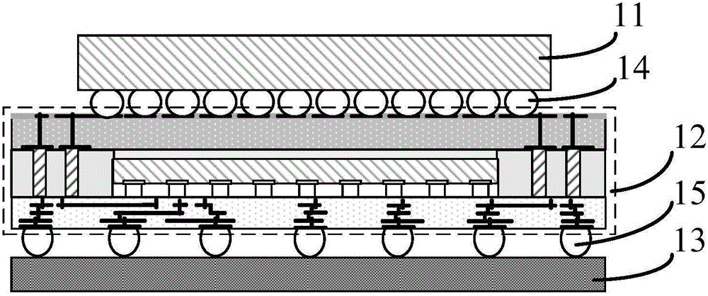
[0122] For ease of understanding, first combine figure 1 The scenario of the chip packaging structure applicable to the embodiment of the present application is briefly described.

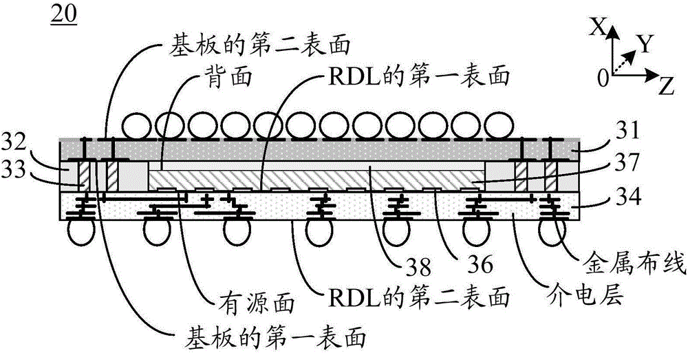
[0123] figure 1 is a schematic diagram of a scenario of a chip packaging structure applicable to an embodiment of the present application. Such as figure 1 As shown, the chip package structure 12 can be connected to the top layer chip 11 through a connector 14 (for example, a solder ball, specifically, a solder ball (solder ball), etc.), and the chip package structure 12 can be connected through a connector 15 ( For example, solder balls (specifically, solderballs, etc.) are connected to a printed circuit board (Printed Circuit Board, “PCB” for short) 13 on the lower layer. Among them, the top chip 11 can be ...


PUM


Abstract

The embodiment of the invention discloses a chip package structure and method. The chip package structure and method can reduce the thickness of the package structure, improve the density of a base pin, add the number of the interconnection channels and increase the bandwidth of the top chip. The chip package structure comprises: a redistribution layer (RDL); a target chip including a source surface and a back surface, wherein the source surface of the target chip is connected with the first surface of the RDL; a substrate, wherein the first surface of the substrate is opposite to the back of the target chip; and an interconnection channel located around the target chip, one end of the interconnection channel is connected with the first surface of the RDL, and the other end of the interconnection channel is connected with the first surface of the substrate.

Description

technical field [0001] The present application relates to the field of chip packaging, and more particularly, to chip packaging structures and methods. Background technique [0002] With the rapid growth of portable electronic products, semiconductor packages mounted on printed circuit boards (Printed Circuit Broad, "PCB" for short) in electronic devices are gradually becoming smaller and thinner. Therefore, the position of packaging in the industry chain has become more important. [0003] At present, there is a known packaging structure, which adopts a package on package (Package on Package, referred to as "POP") technology to package a chip between an upper and a lower substrate. Specifically, the lower substrate can be used to carry the target chip, and the upper substrate can be used to carry the top chip. Through the support of the upper and lower substrates, the stacking of multilayer chip packaging structures in the vertical direction can be realized, thereby realiz...

Claims


Application Information

Patent Timeline
Patent Type & Authority Applications(China)
IPC IPC(8): H01L25/065H01L21/98
CPCH01L25/0657H01L25/50H01L21/568H01L24/19H01L25/105H01L2224/0401H01L2224/04105H01L2224/1132H01L2224/11334H01L2224/11462H01L2224/12105H01L2224/13147H01L2224/16227H01L2224/32225H01L2224/73204H01L2224/73253H01L2224/73267H01L2224/81005H01L2224/92225H01L2224/92244H01L2224/97H01L2225/1035H01L2225/1041H01L2225/1058H01L2225/107H01L2225/1094H01L2924/15192H01L2924/15311H01L2924/1533H01L2924/18161H01L2924/00014H01L2224/83H01L2224/81H01L2224/16225H01L2924/00H01L21/4853H01L21/4857H01L23/3128H01L23/5383H01L23/5386H01L23/5389H01L24/16H01L24/32H01L24/73
Inventor 符会利李珩张晓东
Owner HUAWEI TECH CO LTD
Why Eureka
Try Eureka