Eureka AIR delivers breakthrough ideas for toughest innovation challenges, trusted by R&D personnel around the world.

Chamfering device of optical wafer

A technology of chamfering device and wafer, which is applied in the direction of grinding driving device, grinding machine parts, grinding/polishing equipment, etc., can solve the problems of poor chamfering uniformity, uneven chamfering, and difficult sizing. To achieve the effect of increased adjustment accuracy, easy adjustment, and increased life expectancy

Inactive Publication Date: 2017-04-26
福州紫凤光电科技有限公司
View PDF6 Cites 2 Cited by
  • Summary
  • Abstract
  • Description
  • Claims
  • Application Information

AI Technical Summary

Problems solved by technology

[0002] In the past, the chamfering of optical wafers usually used a simple suction cup to hold the optical parts, and then rolled a circle on the single-axis machine to realize the chamfering of optical wafers. Although this method is low in cost, it is low in efficiency, and the chamfering uniformity is poor. The corner yield is low. In addition, if the centerless edger is used for chamfering, it is also difficult to sizing, resulting in uneven chamfering and low efficiency. It is highly dependent on the operator's technology and proficiency, and the amount of chamfering is manually controlled. It is very difficult, and it is basically impossible to guarantee the same amount of chamfering for different optical components. With the development of automatic assembly of optical modules based on machine vision technology and the continuous increase of labor costs, the chamfering of optical components is increasingly required to have high quality. That is, the amount of chamfering should be precise and the consistency of individual chamfering should be good, which puts forward higher requirements

Method used


Image

  • Chamfering device of optical wafer
  • Chamfering device of optical wafer
  • Chamfering device of optical wafer

Examples


Embodiment Construction

[0024] The following will clearly and completely describe the technical solutions in the embodiments of the present invention in conjunction with the accompanying drawings in the embodiments of the present invention. Obviously, the described embodiments are only preferred embodiments of the present invention, not all embodiments. Based on the embodiments of the present invention, all other embodiments obtained by persons of ordinary skill in the art without creative efforts fall within the protection scope of the present invention.

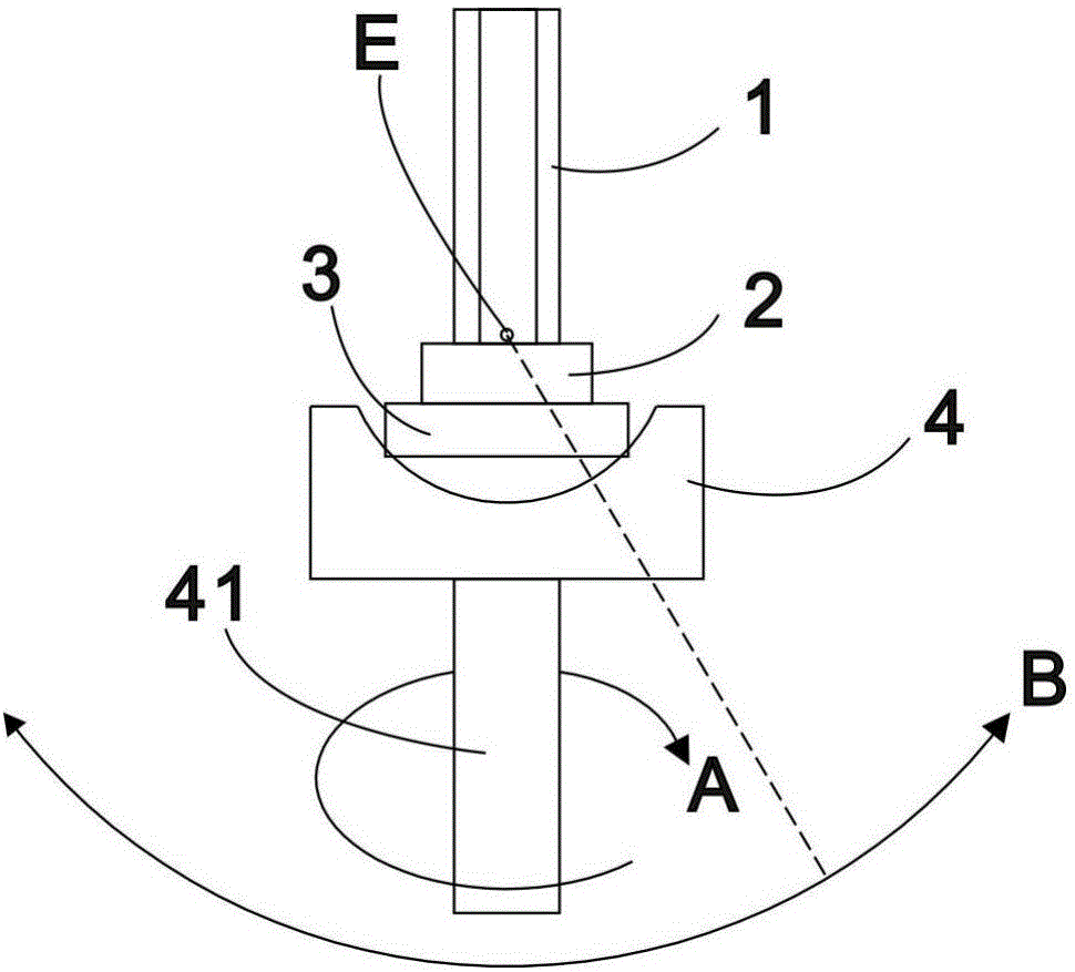
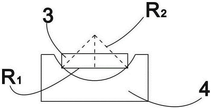
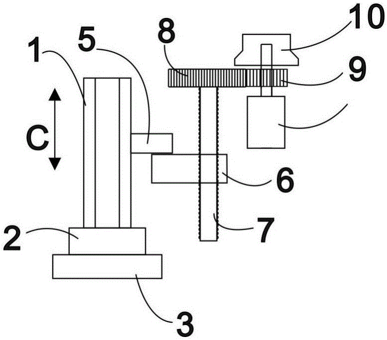
[0025] see figure 1 As shown, a chamfering device for an optical wafer includes a hollow chamfering amount control rod 1, which is a rod with a hollow center structure for controlling the chamfering amount. The tail of the hollow chamfering amount control rod 1 is connected with a vacuum pump (not shown), and the head of the hollow chamfering amount control rod 1 is equipped with a vacuum suction cup 2; Suction the optical wafer 3 to be chamfered...


PUM


Abstract

The invention discloses a chamfering device of an optical wafer. The chamfering device comprises a hollow chamfering amount control rod, wherein the tail of the hollow chamfering amount control rod is connected with a vacuum pump, and a vacuum sucker is mounted at the head of the hollow chamfering amount control rod; a concave bowl piece is arranged below the vacuum sucker, and the inner concave surface of the concave bowl piece is a spherical surface; the concave bowl piece can simultaneously rotate and swing, and the spherical surface center of the concave bowl piece is consistent with the swinging center of the concave bowl piece; and the spherical surface radius of the concave bowl piece is R2, the radius of a to-be-chamfered optical wafer is R1, and the R2 is equal to SQRT(2*R1<2>). The chamfering device can realize the accurate chamfering of the optical wafer with great individual chamfering amount consistency, uniformly grinds the optical wafer, is accurate in chamfering and is high in efficiency.

Description

technical field [0001] The invention relates to an optical precision instrument, in particular to a chamfering device for an optical disc. Background technique [0002] In the past, the chamfering of optical wafers usually used a simple suction cup to hold the optical parts, and then rolled a circle on the single-axis machine to realize the chamfering of optical wafers. Although this method is low in cost, it is low in efficiency, and the chamfering uniformity is poor. The corner yield is low. In addition, if the centerless edger is used for chamfering, it is also difficult to sizing, resulting in uneven chamfering and low efficiency. It is highly dependent on the operator's technology and proficiency, and the amount of chamfering is manually controlled. It is very difficult, and it is basically impossible to guarantee the same amount of chamfering for different optical components. With the development of automatic assembly of optical modules based on machine vision technolo...

Claims


Application Information

Patent Timeline
Patent Type & Authority Applications(China)
IPC IPC(8): B24B9/14B24B47/12B24B41/00B24B41/06
CPCB24B9/14B24B9/146B24B41/00B24B41/002B24B41/06B24B47/12
Inventor 刘承勇
Owner 福州紫凤光电科技有限公司
Why Eureka
Eureka Blog
Learn More