
Silicon micro-flow sensor chip with arrayed cantilever beam membrane structure

A technology of flow sensor and cantilever beam, which is applied in the field of array cantilever beam membrane structure silicon micro-flow sensor chip, can solve the problems of large zero drift, long response time, large power consumption, etc., and achieve improved measurement accuracy, high sensitivity, and small quality Effect

Active Publication Date: 2017-04-26
XI AN JIAOTONG UNIV
View PDF6 Cites 3 Cited by
  • Summary
  • Abstract
  • Description
  • Claims
  • Application Information

AI Technical Summary

Problems solved by technology

However, thermal flow sensors also have their inherent disadvantages, such as large zero drift, high power consumption, and long response time.
At present, the research on non-thermal flow sensors has gradually become the mainstream, but the existing non-thermal flow sensors have problems such as difficulty in taking into account the sensitivity in the full range and complex manufacturing process.

Method used


Image

  • Silicon micro-flow sensor chip with arrayed cantilever beam membrane structure
  • Silicon micro-flow sensor chip with arrayed cantilever beam membrane structure
  • Silicon micro-flow sensor chip with arrayed cantilever beam membrane structure

Examples


Embodiment Construction

[0016] The present invention will be described in detail below in conjunction with the accompanying drawings.

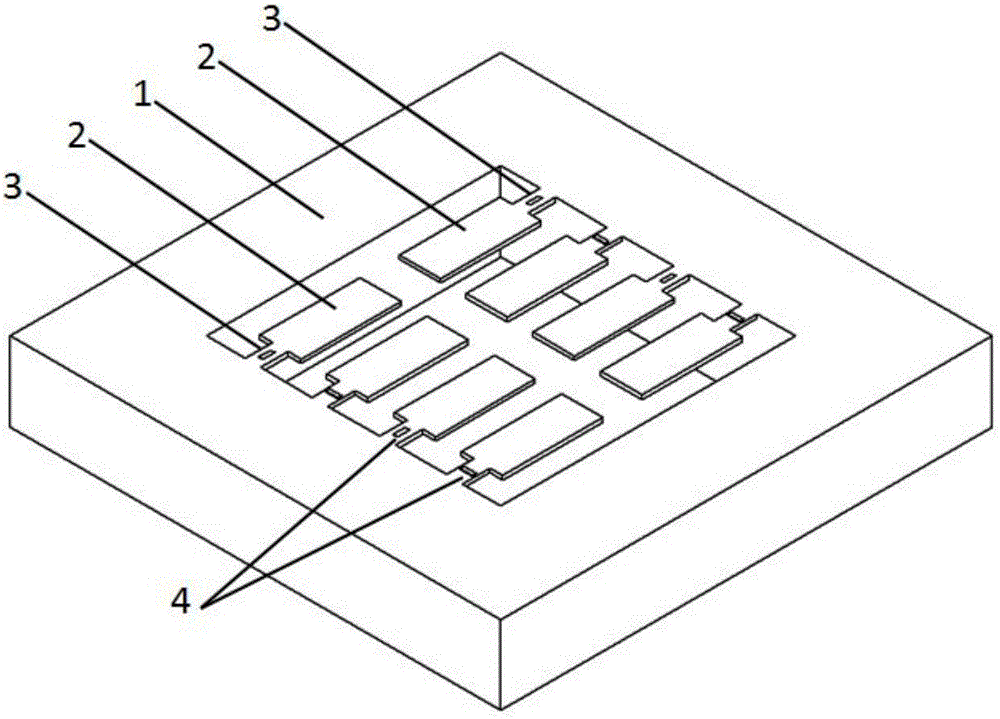
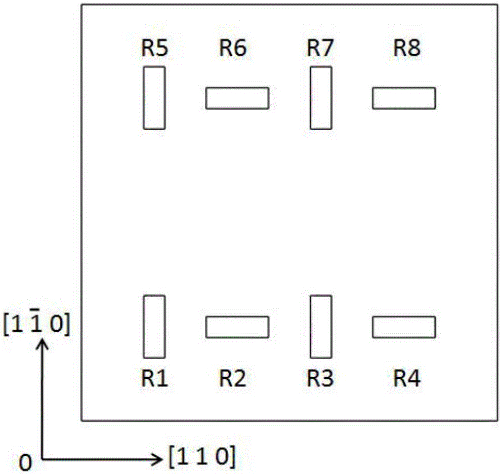
[0017] refer to figure 1 and figure 2 , a silicon microflow sensor chip with an array cantilever beam membrane structure, including a peripheral supporting silicon base 1, and the middle part of the peripheral supporting silicon base 1 is provided with two sets of opposing silicon membranes 2 arranged in an array, and each group has four silicon membranes 2. Each silicon membrane 2 and the peripheral supporting silicon substrate 1 are connected by a silicon cantilever beam 3, and each silicon cantilever beam 3 is equipped with a piezoresistive strip 4, and the four piezoresistive strips of each group of silicon cantilever beams 3 4. The Wheatstone bridge is formed by connecting wires. There are two sets of Wheatstone bridges. The silicon membrane 2 and the silicon cantilever beam 3 are composed of an array cantilever membrane structure to form the sensor measuremen...


PUM


Abstract

A silicon micro-flow sensor chip with an arrayed cantilever beam membrane structure comprises a peripheral supporting silicon substrate, wherein two groups of opposite silicon films which are arranged in an arrayed manner are arranged in the middle of the peripheral supporting silicon substrate; each group has four silicon films; each silicon film is connected with the peripheral supporting silicon substrate through a silicon cantilever beam; each silicon cantilever beam is provided with a piezoresistance strip; the four piezoresistance strips of the silicon cantilever beams of each group are connected through leads to form a wheatstone bridge; the arrayed cantilever beam membrane structure formed by the silicon films and the silicon cantilever beams forms a measurement part of a sensor, a gap is formed between each silicon film and the peripheral supporting silicon substrate so that the silicon film is suspended, a gap is formed between each two adjacent silicon films of each group, when fluid passes through the arrayed cantilever beam membrane structure, the arrayed cantilever beam membrane structure deforms, the resistance value of the piezoresistance strips is changed under the stress effects of the silicon cantilever beams, the wheatstone bridges are out of balance, an electric signal which corresponds to the effect of fluid is output, and therefore, measurement of the flow by the sensor chip is realized. The silicon micro-flow sensor chip with an arrayed cantilever beam membrane structure has the advantages of small size, light weight, high sensitivity and self-calibration ability.

Description

technical field [0001] The invention belongs to the technical field of MEMS flow sensors, in particular to a silicon micro-flow sensor chip with an array cantilever beam membrane structure. Background technique [0002] The measurement of flow parameters is an important task in industrial production and scientific research. With the in-depth research in the field of micro-mechanical electronic systems (MEMS), the flow sensors used to measure flow parameters in fluid flow are developing towards miniaturization, high integration, high precision, and high sensitivity. MEMS flow sensors can be divided into thermal flow sensors and non-thermal flow sensors according to different measurement principles. After long-term development, thermal flow sensors have become the main part of flow sensor research and production. However, thermal flow sensors also have their inherent disadvantages, such as large zero point drift, high power consumption, and long response time. At present, t...

Claims


Application Information

Patent Timeline
IPC IPC(8): G01F1/692
CPCG01F1/692
Inventor 田边李华峰
Owner XI AN JIAOTONG UNIV
Learn More