Silicon chip feeding and calibrating device for photoetching machine and silicon chip feeding and calibrating method

A technology for calibrating devices and lithography machines, which is applied in the direction of photolithography exposure devices, photomechanical equipment, micro-lithography exposure equipment, etc., which can solve the problems of low efficiency of silicon wafer transportation, long waiting time, and failure of silicon wafers. Calibration and positioning and other issues, to achieve the effect of realizing calibration, achieving roundness, and smooth connection

Active Publication Date: 2017-04-26
江苏晋誉达半导体股份有限公司
View PDF6 Cites 7 Cited by
  • Summary
  • Abstract
  • Description
  • Claims
  • Application Information

AI Technical Summary

Problems solved by technology

When the lithography machine performs surface lithography on silicon wafers, it is necessary to take out the silicon wafers from the cassette one by one. At present, most of the silicon wafers are round in shape. Therefore, the silicon wafers only need to be directly fed into the lithography. The position is enough, but the shape of the silicon wafer has changed. In order to facilitate positioning, the edge of the circular silicon wafer is provided with a notch for positioning. One of the positioning notches is an arc-shaped notch. Due to the arc-shaped The existence of the gap requires the silicon wafer to enter the photolithography station in the specified direction to be accurately positioned. However, the current conveying device for the silicon wafer cannot accurately calibrate and position the silicon wafer. Lithography Requirements for Silicon Wafers
[0003] In addition, the feeding efficiency of the current silicon wafers is very low. After the silicon wafers are sent from the wafer pick-up station to the correction station by the silicon wafer conveying device for correction, the silicon wafer conveying device needs to be in the correction station to cooperate with the correction, and it also needs to wait for re-transportation The photolithographic silicon wafer, therefore, the transportation efficiency of the entire working silicon wafer conveying device is very low, and the waiting time is long, which in turn affects the photolithography efficiency of the entire silicon wafer

Method used


Image

  • Silicon chip feeding and calibrating device for photoetching machine and silicon chip feeding and calibrating method
  • Silicon chip feeding and calibrating device for photoetching machine and silicon chip feeding and calibrating method
  • Silicon chip feeding and calibrating device for photoetching machine and silicon chip feeding and calibrating method

Examples


Embodiment Construction

[0042] The present invention will be described in further detail below through specific examples.

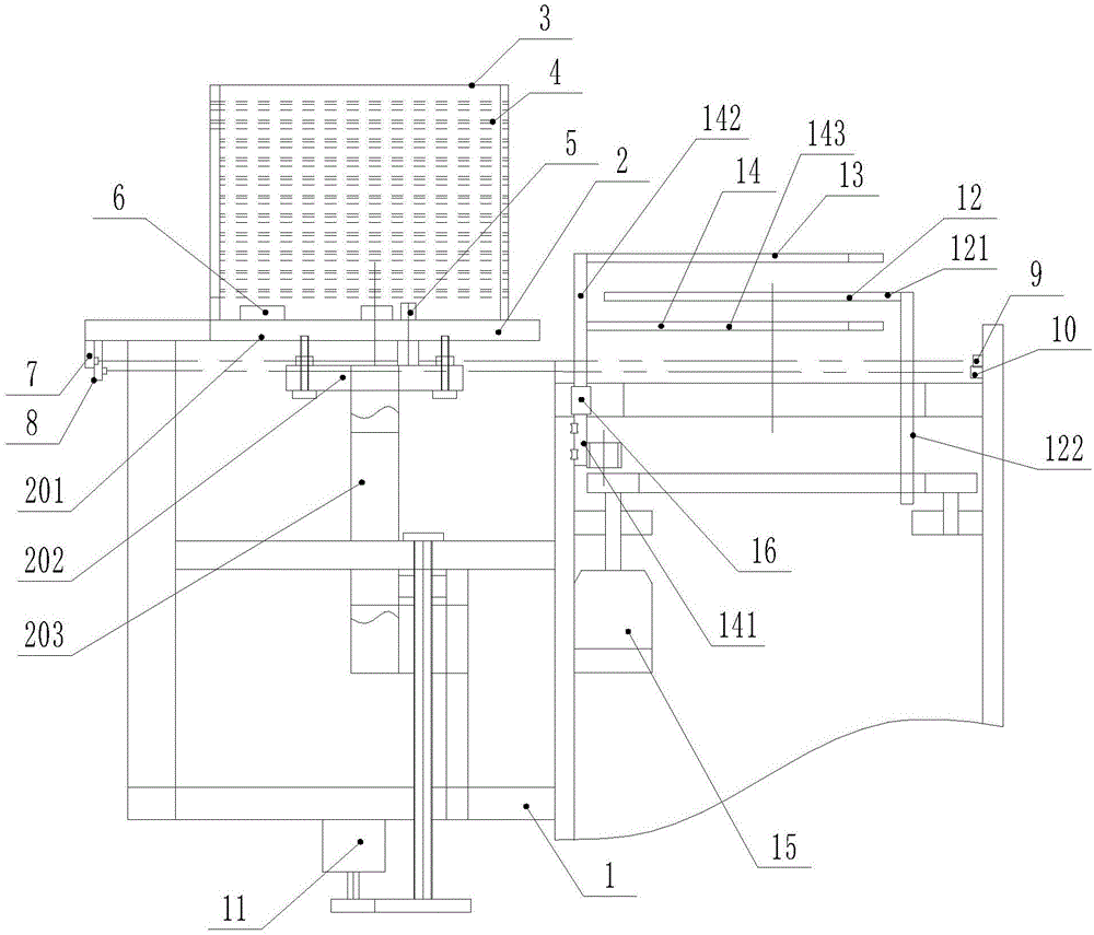
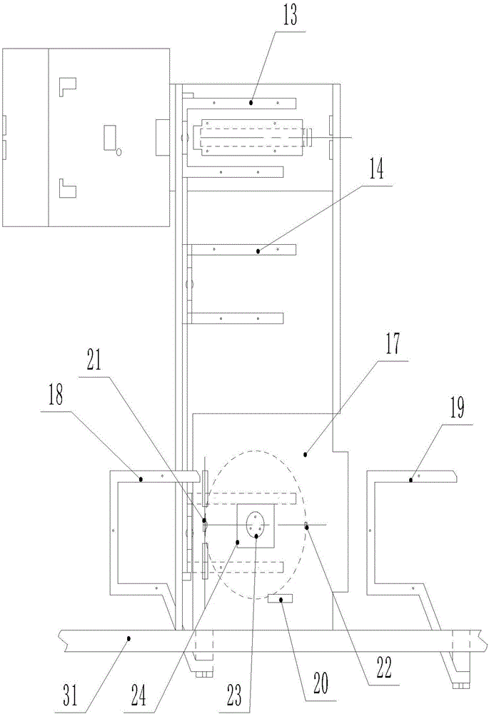
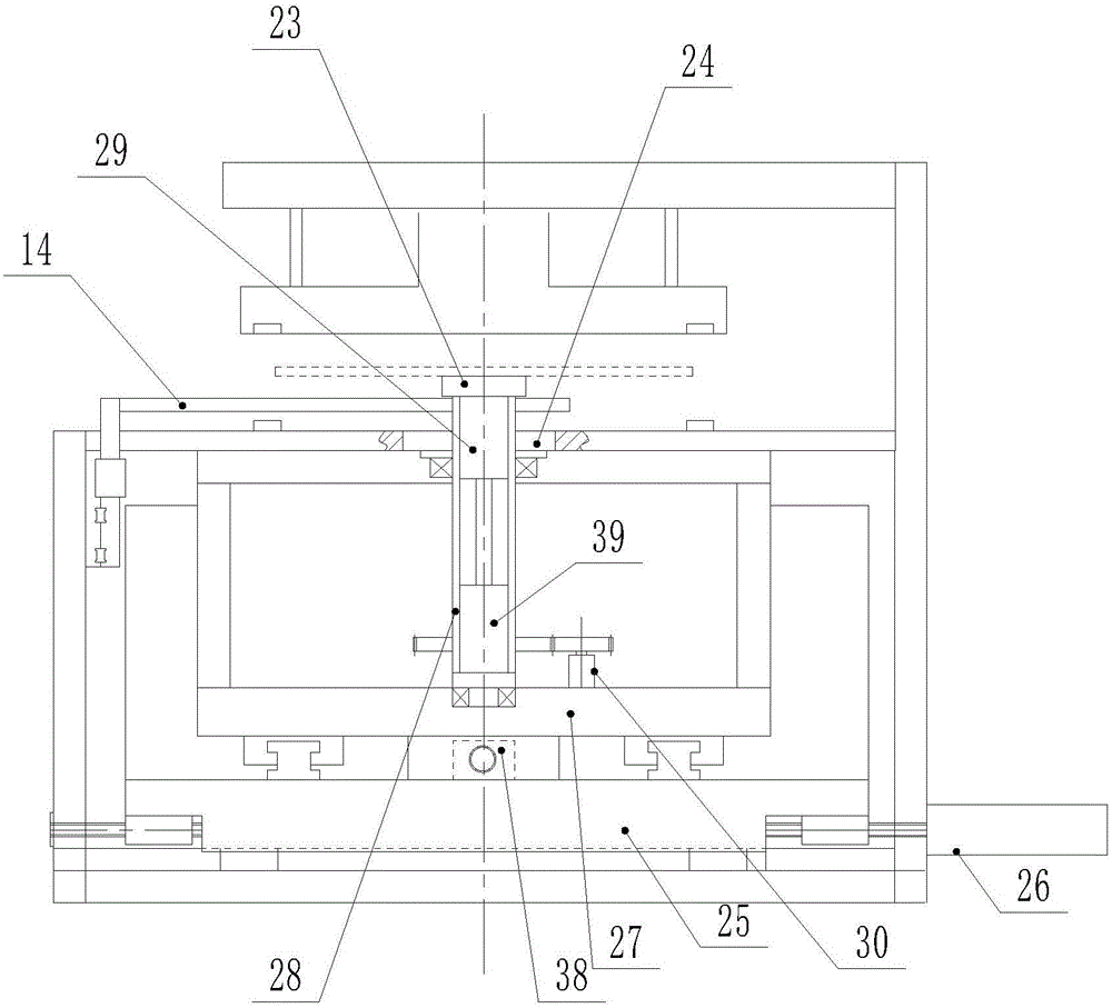
[0043] Such as Figure 1 to Figure 5 As shown, a silicon wafer feeding calibration device for a lithography machine includes a frame on which a lifting seat for placing a cassette is vertically slidably installed, and the lifting seat is driven and connected by a first lifting power device , the lifting seat includes a placement platform, a connecting base and a vertical seat, the placing platform is fixed on the upper end of the connecting base, the connecting base is fixed on the upper end of the vertical seat, and the vertical seat is vertically slidably installed on the machine through guide rails. On the shelf, the vertical seat is connected to the first lifting power device in transmission, and the positioning boss corresponding to the bottom of the film box is arranged on the said placing platform, and a contact switch is also arranged on the placing platform, and only th...


PUM


Abstract

The invention discloses a silicon chip feeding and calibrating device for a photoetching machine and a silicon chip feeding and calibrating method. The silicon chip feeding and calibrating device can take silicon chips out from a silicon chip box one by one and then convey the silicon chips to a calibration station by using a first transmission rack and a second transmission rack alternately; then the silicon chip feeding and calibrating device carries out rapid calibration at the calibration station by using at least three circumference-calibrating through-beam sensors, a rough detection sensor and a fine detection sensor so as to ensure that the circle centers and gaps of the silicon chips are located at assigned positions; and a first transferring rack and a second transferring rack are alternately used for conveying the silicon chips to a photoetching station for photoetching so as to ensure accurate positioning and photoetching of the silicon chips having entered the photoetching station. The silicon chip feeding and calibrating device and the silicon chip feeding and calibrating method save time, improve efficiency and are accurate in calibration and high in calibration precision.

Description

technical field [0001] The invention relates to a feeding calibration device, which is used for feeding calibration of a silicon wafer of a photolithography machine to facilitate photolithography, and meanwhile, the invention also relates to a feeding calibration method of the photolithography machine. Background technique [0002] In the production process of integrated circuit chips, the exposure transfer (photolithography) of the design pattern of the chip on the photoresist on the surface of the silicon wafer is one of the most important processes. The equipment used in this process is called a photolithography machine (exposure machine). Lithography machine is the most critical equipment in the process of integrated circuit processing. When the lithography machine performs surface lithography on silicon wafers, it is necessary to take out the silicon wafers from the cassette one by one. At present, most of the silicon wafers are round in shape. Therefore, the silicon w...

Claims


Application Information

Patent Timeline
Patent Type & Authority Applications(China)
IPC IPC(8): G03F7/20G03F9/00
CPCG03F7/70733G03F9/7049
Inventor 丁桃宝
Owner 江苏晋誉达半导体股份有限公司
Why Eureka
Try Eureka