Method of preparing ultrathin silicide

A silicide, ultra-thin technology, used in semiconductor/solid-state device manufacturing, semiconductor devices, electrical components, etc., can solve the problems of secondary annealing temperature not too high, different annealing temperatures in different regions, interface spikes, etc. The effect of requirements, low cost and simple process

Inactive Publication Date: 2017-05-03
PEKING UNIV
View PDF6 Cites 4 Cited by
  • Summary
  • Abstract
  • Description
  • Claims
  • Application Information

AI Technical Summary

Problems solved by technology

However, the former has higher requirements on the thickness and uniformity of the deposited metal; the characteristic of the latter is that in order to form ultra-thin silicide, the temperature and time of the initial annealing must be strictly controlled to control the amount of metal driven i

Method used


Image

  • Method of preparing ultrathin silicide
  • Method of preparing ultrathin silicide
  • Method of preparing ultrathin silicide

Examples


Embodiment Construction

[0029] The present invention will be described in detail below in conjunction with the accompanying drawings and specific examples.

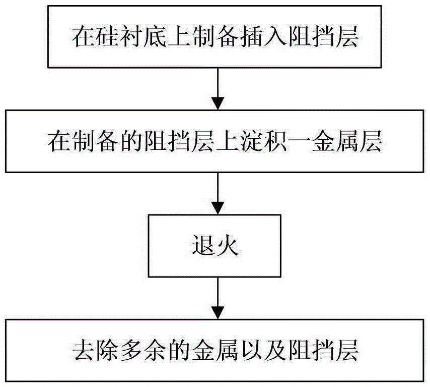
[0030] Process flow of the present invention such as figure 1 As shown, the preparation of ultra-thin nickel silicide can be realized according to the following steps:

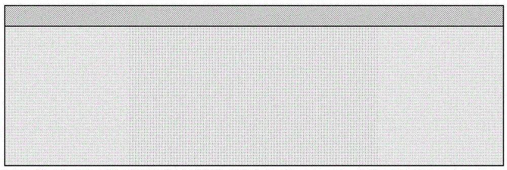
[0031] 1) ALD on a 4-inch N-type (100) bulk silicon substrate Al 2 o 3 As an insertion barrier, such as figure 2 shown;

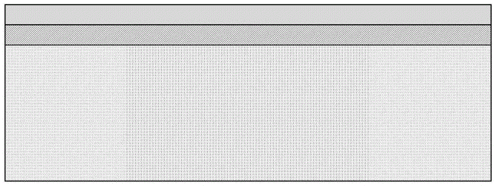
[0032] 2) Sputter 50nm metallic Ni. Such as image 3 shown;

[0033] 3) Perform rapid thermal annealing at 600°C for 10 minutes, metal Ni diffuses through the insertion barrier layer and reacts with silicon to form NiSi 2 ,Such as Figure 4 shown;

[0034] 4) Use the ratio of H 2 SO 4 :H 2 o 2 = 4:1 solution to remove unreacted Ni and Al 2 o 3 , the corrosion time is 10min, such as Figure 5 shown;

[0035] Ultimately achieve ultra-thin NiSi with a thickness of less than 2nm 2 preparation.

[0036] The embodiments of the present inventio...


PUM


Abstract

The invention discloses a method of preparing an ultrathin silicide. The method comprises the following steps: (1) preparing an insertion stop layer on a silicon substrate; (2) preparing a metal layer on the stop layer; (3) annealing the structure obtained in step (2) to make metal in the metal layer diffuse across the insertion stop layer and react with silicon to form an ultrathin silicide; and (4) removing excess metal and the insertion stop layer to get an ultrathin silicide. Through the method, an ultrathin silicide less than 2nm can be prepared. The amount of metal driven in is controlled by changing the thickness of the insertion stop layer, so that silicides made of the same metal but of different phases and thicknesses can be obtained. The process is of high controllability. The formed ultrathin silicide has the characteristics of low resistivity, low Schottky barrier, good uniformity, and good smoothness. Compared with the conventional ultrathin silicide preparation method, the meal deposition process window is widened greatly. The method is completely compatible with a bulk silicon CMOS process. The process is simple and low in cost.

Description

technical field [0001] The invention belongs to the technical field of ultra-large-scale integrated circuit manufacturing, and relates to a method for preparing ultra-thin metal silicide in integrated circuits. Background technique [0002] When the process node of integrated circuits advances to 14nm, traditional planar transistors face many problems such as serious short-channel effects and performance degradation, and can no longer meet the requirements of proportional scaling. Multi-gate devices enhance the coupling ability between the gate and the channel by increasing the number of gates, which has become the mainstream of logic devices in the post-Moore era. Due to the continuous shrinking of the size, the proportion of the source-drain resistance in the total resistance is increasing, and the on-state current of multi-gate devices is seriously degraded. Therefore, reducing the source-drain parasitic resistance is very important for optimizing the on-state performance...

Claims


Application Information

Patent Timeline
IPC IPC(8): H01L21/28
CPCH01L21/28518
Inventor 黎明陈珙杨远程张昊樊捷闻黄如
Owner PEKING UNIV
Why Eureka
Try Eureka