
MOS transistor device

A technology of MOS tubes and devices, which is applied in the field of metal oxide semiconductor devices, can solve the problems of poor isolation ability, voltage swing blocking ability, and affecting the device’s ability to turn off AC signals, so as to improve the turn-off ability, Effects of improving impedance and breakdown voltage

Inactive Publication Date: 2017-05-03
INNOGRATION SUZHOU
View PDF2 Cites 1 Cited by
  • Summary
  • Abstract
  • Description
  • Claims
  • Application Information

AI Technical Summary

Problems solved by technology

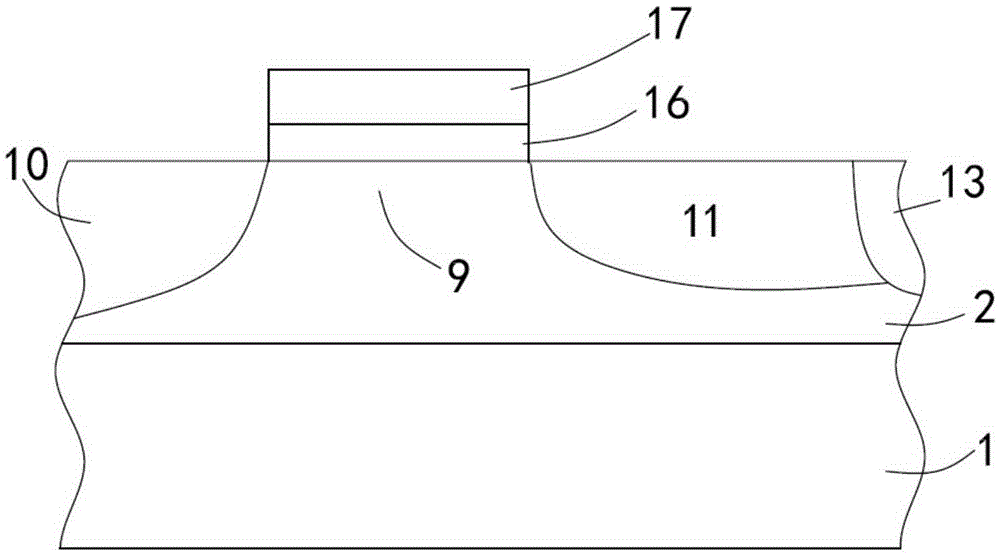
However, in fact, when the tube is in the on state, the drain-source on-resistance Rdson is a fixed quantity, and affected by the LDD region, the drain-source on-resistance Rdson and the drain-source capacitance Cds become a pair of quantities that are difficult to reconcile. The reason is as follows: In order to reduce the on-resistance Rdson of the device, the length of the LDD region needs to be reduced to reduce the distance between the source region and the drain region, so that the drain-source capacitance Cds of the device in the off state is bound to increase Larger, so that the impedance between the drain and the source is reduced, resulting in poor isolation between the source and the drain, and at the same time, the device's ability to block the voltage swing is also poor, and ultimately not only affects the device's ability to turn off the AC signal ability, and also reduces the breakdown voltage BVdss, resulting in an increased risk of device breakdown

Method used


Image

  • MOS transistor device
  • MOS transistor device
  • MOS transistor device

Examples


Embodiment Construction

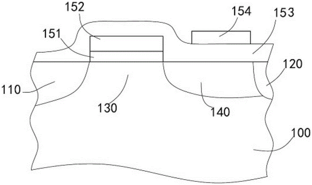
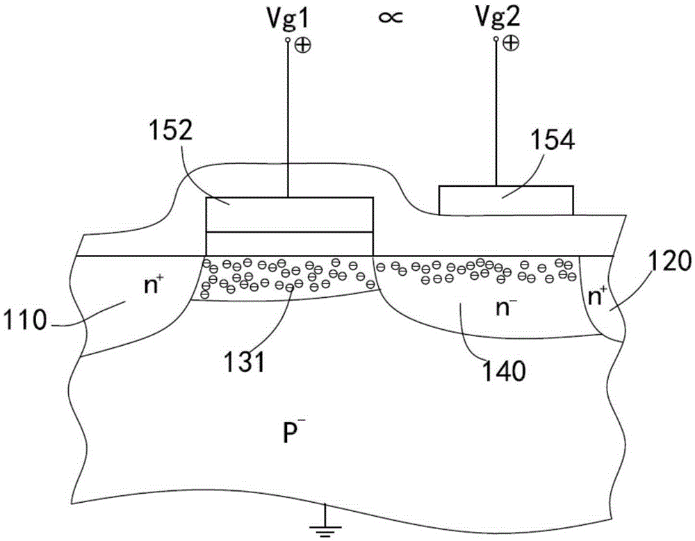
[0023] As mentioned in the background technology, for the existing MOS devices, the device is required to have the lowest possible drain-source on-resistance Rdson when it is working, so as to reduce the current consumption of the device and improve the response speed of the device. In the off state, the drain and source have the lowest possible drain-source capacitance Cds and the highest possible impedance, so that the device will not generate leakage and loss. However, in fact, when the tube works in the saturation region, the drain-source on-resistance Rdson is a fixed quantity, and affected by the LDD region, the drain-source on-resistance Rdson and the drain-source capacitance Cds become a pair of quantities that are difficult to reconcile. The reason is as follows: In order to reduce the on-resistance Rdson of the device, the length of the LDD region needs to be reduced to reduce the distance between the source region and the drain region, so that the drain-source capaci...


PUM


Abstract

The invention discloses an MOS transistor device. The MOS transistor device is provided with two gates, the first gate is a common gate arranged above a channel for controlling on and off of the device, and the second gate is a newly-added gate arranged above an LDD area for controlling drain-source on resistance Rdson. Through regulation by the second gate, on one hand, when the device is in a working state, the drain-source on resistance Rdson can be reduced, thereby reducing the working loss of the device and improving the on-off efficiency, and on the other hand, when the device is in an off state, drain-source capacitance Cds is reduced, the impedance between the drain and the source and the breakdown voltage BVdss are improved, and the separation ability when the device is off and the voltage swing blocking ability are thus improved.

Description

technical field [0001] The invention relates to a metal oxide semiconductor device, in particular to a metal oxide semiconductor device with a double gate structure. Background technique [0002] With the improvement of integrated circuit integration, the device size is gradually reduced in proportion, and the current feature size has reached the order of 32nm. Metal-oxide-semiconductor (MOS) is the most common semiconductor device and is the basic unit of various complex circuits. The basic structure of a MOS transistor includes three main regions: source, drain, and gate. The source and drain are formed by high doping, which can be divided into n-type doping (NMOS) and p-type doping (PMOS) according to different device types. [0003] In the process of scaling down the device, the drain voltage does not decrease accordingly, which leads to an increase in the electric field in the channel region between the source / drain, under the action of a strong electric field, electr...

Claims


Application Information

Patent Timeline
Patent Type & Authority Applications(China)
IPC IPC(8): H01L29/78
CPCH01L29/7833H01L29/7831
Inventor 马强
Owner INNOGRATION SUZHOU
Learn More