
Wafer discharging method, wafer discharging auxiliary device, wafer discharging device and CMP equipment comprising wafer discharging device

An auxiliary device and wafer technology, which is applied in the direction of grinding devices, metal processing equipment, grinding/polishing equipment, etc., can solve the problems of wafer loss, normal production and production profit impact, and reduce production capacity and efficiency. Prevent being scratched and broken, improve productivity and efficiency, improve productivity and efficiency

Active Publication Date: 2017-05-10
HWATSING TECH +1
View PDF6 Cites 9 Cited by
  • Summary
  • Abstract
  • Description
  • Claims
  • Application Information

AI Technical Summary

Problems solved by technology

Once a wafer is scratched or broken, the machine must be shut down for cleaning, consumables must be replaced and maintenance and testing will be performed, which will result in the loss of damaged wafers. At the same time, the production capacity and efficiency will be reduced. Normal production and production profits have a great impact

Method used


Image

  • Wafer discharging method, wafer discharging auxiliary device, wafer discharging device and CMP equipment comprising wafer discharging device
  • Wafer discharging method, wafer discharging auxiliary device, wafer discharging device and CMP equipment comprising wafer discharging device
  • Wafer discharging method, wafer discharging auxiliary device, wafer discharging device and CMP equipment comprising wafer discharging device

Examples


Embodiment Construction

[0045] Embodiments of the invention are described in detail below, examples of which are illustrated in the accompanying drawings. The embodiments described below with reference to the accompanying drawings are exemplary, intended to explain the present invention, but not to be construed as limitations of the present invention, those skilled in the art can change the above-mentioned embodiments within the scope of the present invention , modification, substitution and variation.

[0046] In describing the present invention, it is to be understood that the terms "center", "upper", "lower", "vertical", "horizontal", "top", "bottom", "inner", "outer", The orientations or positional relationships indicated by "axial", "radial", and "circumferential" are based on the orientations or positional relationships shown in the drawings, and are only for the convenience of describing the present invention and simplifying the description, rather than indicating or implying the It should no...


PUM


Abstract

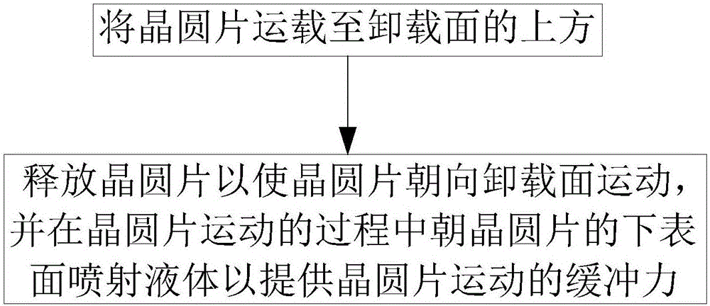
The invention discloses a wafer discharging method, auxiliary device and device, and CMP equipment comprising the wafer discharging device. The wafer discharging method comprises the following steps of conveying a wafer to the position above a discharge surface; releasing the wafer to enable the wafer to move towards the discharge surface; spraying liquid to the lower surface of the wafer in the moving process of the wafer to provide buffering force for the moving wafer. According to the wafer discharging method provided by the embodiment of the invention, the wafer can be prevented from being scratched and broken during wafer discharging; accordingly, the yield of wafers can be increased, the productivity and efficiency can be improved, the frequency of shutdown maintenance can be reduced, and the cost can be lowered.

Description

technical field [0001] The present invention relates to the technical field of chemical machinery, more specifically, to a wafer unloading method, a wafer unloading auxiliary device, a wafer unloading device and a CMP with a wafer unloading device equipment. Background technique [0002] In the semiconductor integrated circuit chip manufacturing process, planarization technology has become one of the indispensable key technologies that are equally important and interdependent with photolithography and etching. The chemical mechanical polishing (CMP) process is currently the most effective and mature planarization technology. The chemical mechanical polishing system is a chemical mechanical planarization technology integrating polishing, cleaning, drying, online detection, end point detection and other technologies. CMP equipment is fully automated and does not require manual operation to ensure the safety of each module and link in the production process of the wafer. It i...

Claims


Application Information

Patent Timeline
Patent Type & Authority Applications(China)
IPC IPC(8): B24B37/34B24B55/00H01L21/677
CPCB24B37/345B24B55/00H01L21/67739
Inventor 孙浩明路新春雒建斌温诗铸王同庆李昆沈攀
Owner HWATSING TECH
Learn More