Technology mapping method by utilizing carry chain

A carry chain and carry output technology, applied in the field of process mapping using carry chain, can solve problems such as long delay and multiple logic resources, and achieve the effect of reducing delay and saving logic resources.

Active Publication Date: 2017-05-10
CAPITAL MICROELECTRONICS
View PDF3 Cites 2 Cited by
  • Summary
  • Abstract
  • Description
  • Claims
  • Application Information

AI Technical Summary

Problems solved by technology

However, for the AND and OR logic of a longer width, this implementation method using a lookup table will take up more logic resources and require a longer delay.

Method used


Image

  • Technology mapping method by utilizing carry chain
  • Technology mapping method by utilizing carry chain
  • Technology mapping method by utilizing carry chain

Examples


Embodiment Construction

[0027] In order to make the purpose, technical solutions and advantages of the embodiments of the present invention clearer, the technical solutions in the embodiments of the present invention will be clearly and completely described below in conjunction with the drawings in the embodiments of the present invention. Obviously, the described embodiments It is a part of embodiments of the present invention, but not all embodiments.

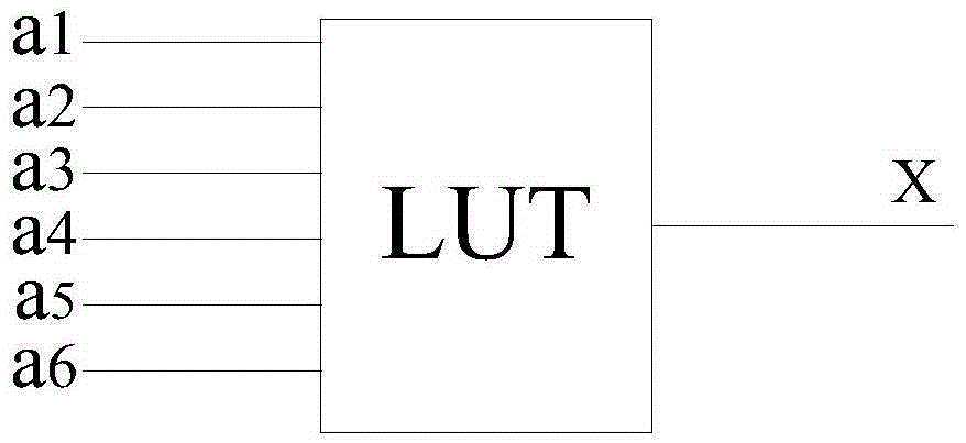
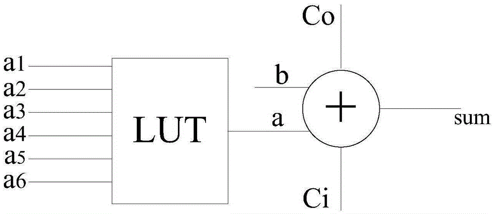
[0028] The invention provides a process mapping method using carry chains. The present invention realizes the process mapping of longer-width AND-OR logic by using a process mapping method combining a look-up table and an adder, which can save chip logic resources and greatly reduce the delay in realizing the logic.

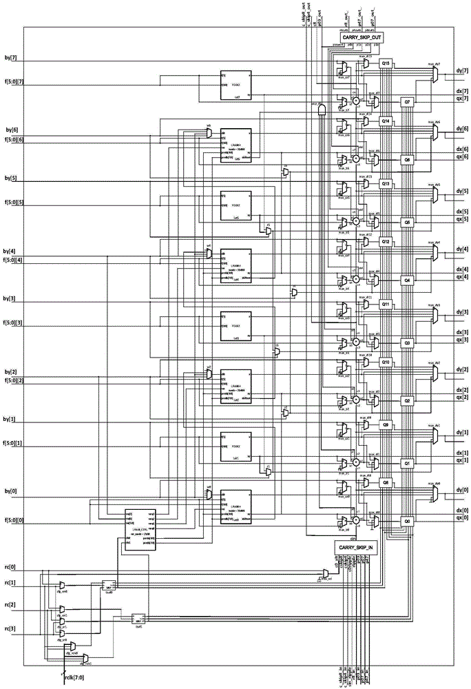
[0029] The methods in the following embodiments of the present invention are realized based on the CME-C1 series FPGA devices. To better understand the technical solutions provided by the embodiments of the present invention, the archi...


PUM


Abstract

The invention relates to a technology mapping method by utilizing a carry chain. According to the method, an FPGA comprises multiple logical units, and one logical unit comprises multiple logical pieces; the output end of a multi-input lookup table in a logical piece LP on a logical element LE of the FPGA is connected to the input end of a second addend of a first summator; one bit signal is input to the carry input end of the first summator and one bit signal is input to the input end of a first addend; a carry output signal is output through the carry output end of the first addend. According to the technology mapping method by utilizing the carry chain, by utilizing the technology mapping method which combines the lookup table and the addend, technology mapping with a long width and / or logic is achieved, chip logical resources can be saved, and time delaying of achieving the logic can be sharply reduced at the same time.

Description

technical field [0001] The invention relates to the technical field of integrated circuit design in the field of microelectronics, in particular to a process mapping method using carry chains. Background technique [0002] FPGA is a logic device with abundant hardware resources, powerful parallel processing capability and flexible reconfigurable capability. These features make FPGA more and more widely used in data processing, communication, network and many other fields. [0003] Currently, in Field Programmable Gate Array (Field Programmable Gate Array, FPGA) applications, integrated circuits are required to have a programmable or configurable interconnection network, and logic gates are connected to each other through the configurable interconnection network. FPGAs, functioning as stand-alone chips or as a core part of a system, have been widely used in a large number of microelectronic devices. The definition of FPGA logic gates in a broad sense not only refers to simp...

Claims


Application Information

Patent Timeline
Patent Type & Authority Applications(China)
IPC IPC(8): G06F17/50
CPCG06F30/39Y02D10/00
Inventor 耿嘉
Owner CAPITAL MICROELECTRONICS
Why Eureka
Try Eureka