Semiconductor device voltage-withstanding structure

A voltage-resistant structure, semiconductor technology, applied in the direction of semiconductor devices, electrical components, circuits, etc.

Active Publication Date: 2017-05-10
CSMC TECH FAB2 CO LTD
View PDF3 Cites 21 Cited by
  • Summary
  • Abstract
  • Description
  • Claims
  • Application Information

AI Technical Summary

Problems solved by technology

In the traditional method, the breakdown voltage of the entire semiconductor device withstand voltage structure 100 is increased by increasing the thickness of the dielectric layer 107 and the field oxide layer 106. However, this method has limitations in the application of high voltage and ultra-high voltage, generally only Applied to semiconductor devices with working voltage lower than 300V

Method used


Image

  • Semiconductor device voltage-withstanding structure
  • Semiconductor device voltage-withstanding structure
  • Semiconductor device voltage-withstanding structure

Examples


Embodiment Construction

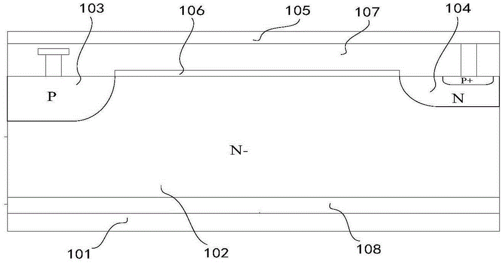
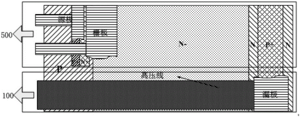
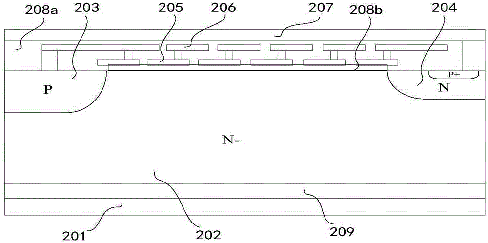
[0027] In order to more clearly explain the withstand voltage structure of the semiconductor device provided by the present invention, the specific description will be given below in conjunction with the embodiments. In the following embodiments, the withstand voltage structure of the semiconductor device is provided in the semiconductor device to increase the breakdown voltage of the semiconductor device, and the laterally diffused metal oxide semiconductor is taken as an example for illustration.

[0028] The voltage-resistant structure of a semiconductor device provided by the present invention includes a high-voltage interconnection area for arranging high-voltage interconnection lines, and the lower part of the high-voltage interconnection area is a metal layer, a dielectric layer, a field oxide layer, and a drift area other than the active area. , the withstand voltage structure of the semiconductor device further includes a plurality of conductor field plates and a plura...


PUM


Abstract

The invention relates to a semiconductor device voltage-withstanding structure. The semiconductor device voltage-withstanding structure comprises a high-voltage interconnection area used for arranging a high-voltage interconnection line, and a metal layer, a dielectric layer, a field oxide layer and an area, apart from an active region, of a drift area are successively arranged below the high-voltage interconnection area. The semiconductor device voltage-withstanding structure further comprises a plurality of conductor field plates and a plurality of semi-insulating resistor filed plates, wherein the conductor field plates are disposed above the semi-insulating resistor filed plates, and the conductor field plates are disposed in the dielectric layer, all the semi-insulating resistor filed plates are adjacent to the field oxide layer, the conductor field plates and the semi-insulating resistor filed plates form a plurality of capacitors, and any one capacitor at least can transmit energy to another capacitor. The semiconductor device voltage-withstanding structure generally reduces high voltages borne by the surface of the drift area, improves breakdown voltages of a semiconductor device and enables the semiconductor device to work under higher voltages.

Description

technical field [0001] The invention relates to the technical field of semiconductor devices, in particular to a voltage-resistant structure of a semiconductor device. Background technique [0002] In a semiconductor device, if it needs to work at a higher voltage, it is necessary to connect a part of the electrodes to the peripheral high-voltage busbar through a high-voltage interconnection line. If the high-voltage interconnection line contains an active area under the area covered by the surface of the semiconductor device, when the high-voltage interconnection line is connected to the high-voltage bus bar, the high voltage will be transmitted to the active area through the contact hole through the dielectric layer and the field oxide layer, which may This leads to breakdown in the active region and ultimately makes the entire semiconductor device ineffective. Therefore, for a semiconductor device that needs to work at a higher voltage, an area dedicated to arranging the...

Claims


Application Information

Patent Timeline
Patent Type & Authority Applications(China)
IPC IPC(8): H01L29/40H01L29/78H01L29/861H01L29/739
Inventor 顾炎宋华张森
Owner CSMC TECH FAB2 CO LTD
Why Eureka
Try Eureka