High density low voltage trench power MOS device and method of manufacturing same

A technology of MOS devices and manufacturing methods, applied in semiconductor/solid-state device manufacturing, semiconductor devices, electrical components, etc., can solve problems such as cost increase and 8-inch fab equipment cost increase, and reduce characteristic on-resistance, reduce The minimum unit cell width and the effect of increasing the cell density

Pending Publication Date: 2017-05-10
YANGZHOU YANGJIE ELECTRONIC TECH CO LTD
View PDF3 Cites 7 Cited by
  • Summary
  • Abstract
  • Description
  • Claims
  • Application Information

AI Technical Summary

Problems solved by technology

If you want to change this limitation, you need to purchase an extremely expensive lithography machine with higher precision

Method used


Image

  • High density low voltage trench power MOS device and method of manufacturing same
  • High density low voltage trench power MOS device and method of manufacturing same
  • High density low voltage trench power MOS device and method of manufacturing same

Examples


Embodiment Construction

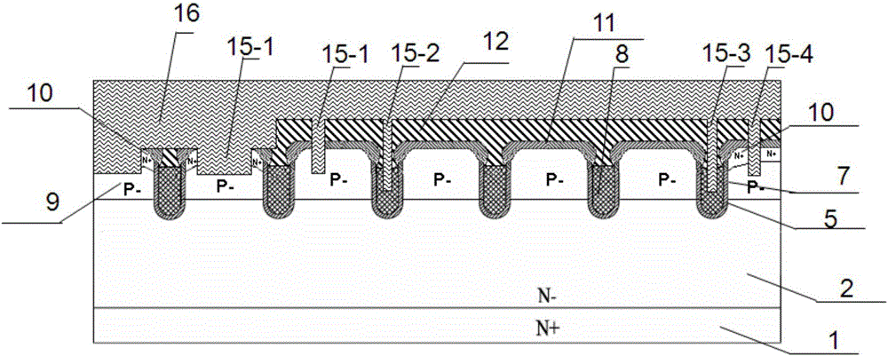
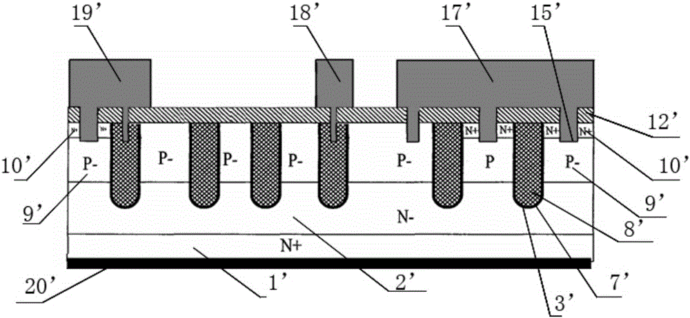
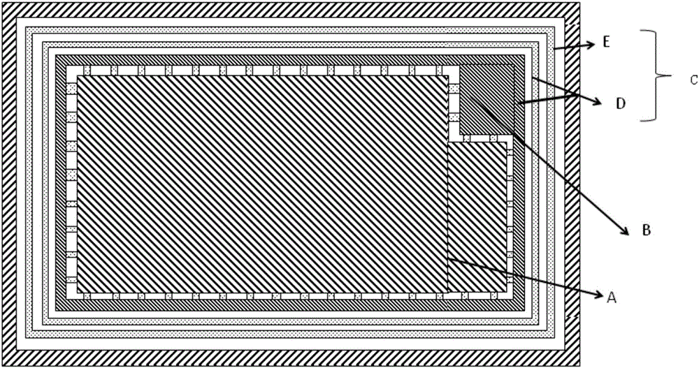
[0080] In order to make the above objects, features and advantages of the present invention more comprehensible, the specific implementation manners of the present invention will be further described below in conjunction with specific drawings.

[0081] In the following description, a lot of specific details are set forth in order to fully understand the present invention, but the present invention can also be implemented in other ways that are different from those described here, and those skilled in the art can do so without departing from the connotation of the present invention. By analogy, the present invention is not limited by the specific examples disclosed below.

[0082] Secondly, the present invention is described in detail in combination with schematic diagrams. When describing the embodiments of the present invention in detail, for the convenience of explanation, the cross-sectional view showing the device structure will not be partially enlarged according to the g...


PUM

PropertyMeasurementUnit
Thicknessaaaaaaaaaa

Abstract

The invention relates to a high density low voltage trench power MOS device and a method of manufacturing the same. A bowl structure of a trench is formed by performing thermal oxidation (a thickness of 500A-5000A) to the upper part of the trench, and a dry general etching method of a high selection ratio (silicon dioxide: silicon) is also selected for etching only silicon under the premise of not etching silicon dioxide, so that the etching of a contact hole in a cellular region of a trench power MOS device is realized, also known as self-aligned etching of the contact hole. Meanwhile, the invention also achieves the etching of a lead-out hole in a terminal protection region of the device, without increasing apparent process steps. As is well known in the industry, for self-aligned etching, the registration deviation of lithography can be considered to be zero. In this way, in the current 8-inch fab lithography machine operation, the invention can greatly reduce the cellular width of a minimum cell of the cellular region from 0.9 <mu>m to 0.5 <mu>m, thus greatly improving the cellular density (an integration degree) and reducing the overall specific on-resistance.

Description

technical field [0001] The invention relates to a high-density low-voltage trench power MOS device and a manufacturing method thereof, belonging to the technical field of semiconductors. Background technique [0002] For existing trench power MOSFET devices, for products with a voltage between positive (negative) 8V-100V, because the application side mainly pursues low characteristic on-resistance, it is hoped that the design can increase the density of cells as much as possible to realise. Such as figure 1 As shown, it is a schematic structural diagram of a traditional low-voltage trench power MOS device, including N+ substrate 1', N- epitaxial layer 2', trench 3', gate oxide layer 7', conductive polysilicon 8', P-well Region 9', N+ source 10', dielectric layer 12', contact hole 15', source metal 17', gate metal 18', terminal stop ring metal 19' and back metal layer 20'. [0003] The traditional low-voltage trench power MOS device, the manufacturing method includes the f...

Claims


Application Information

Patent Timeline
IPC IPC(8): H01L29/417H01L29/423H01L29/78H01L21/336H01L21/28
CPCH01L29/41741H01L29/4236H01L29/66666H01L29/7827
Inventor 周祥瑞冷德武王毅
Owner YANGZHOU YANGJIE ELECTRONIC TECH CO LTD
Why Eureka
Try Eureka