Preparation method for copper-indium-tellurium ultrathin regular semiconductor nanosheets

A technology of copper indium tellurium and nanosheets, which is applied in the fields of nanotechnology, nanotechnology, nanotechnology for materials and surface science, etc., can solve the problems of limited synthesis difficulty and insignificant results.

Inactive Publication Date: 2017-05-17
OCEAN UNIV OF CHINA
View PDF7 Cites 0 Cited by
  • Summary
  • Abstract
  • Description
  • Claims
  • Application Information

AI Technical Summary

Problems solved by technology

CuInTe 2 It also belongs to I-III-VI semiconductor nanomaterials, and also has the above-mentioned advantages, but is limited by its own synthesis difficulty. Although its preparation and application have attracted widespread attention in the scientific community, the results achieved are not significant.

Method used


Image

  • Preparation method for copper-indium-tellurium ultrathin regular semiconductor nanosheets
  • Preparation method for copper-indium-tellurium ultrathin regular semiconductor nanosheets
  • Preparation method for copper-indium-tellurium ultrathin regular semiconductor nanosheets

Examples


Embodiment Construction

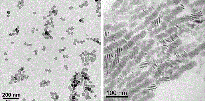
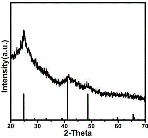
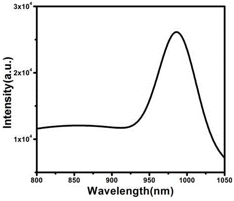
[0006] During operation, first weigh a certain amount of precursors of copper source and indium source, dissolve them in an eighteen-dilute solution adding a certain amount of surface ligands, and form an organic solution of about 0.02mol / L, and then degas and fill The mixed solution was heated to 90°C while alternating the inert gas. Weigh a certain amount of tellurium powder and add it into the organic solution to form a 0.5mol / L tellurium-containing organic solution, and promote the dissolution of the tellurium powder by heating, then add it to the previous mixed solution, and keep stirring. Then degas a certain amount of eighteen dilute solvent at 120°C, and then raise the temperature to a higher temperature, quickly inject the final mixed solution into the eighteen dilute solvent at high temperature, then stop the reaction, and quickly cool down At room temperature, ultrathin regular nanosheets of copper indium tellurium are obtained. The method of collecting copper indi...


PUM

PropertyMeasurementUnit
sizeaaaaaaaaaa
sizeaaaaaaaaaa

Abstract

The invention discloses a preparation method for copper-indium-tellurium ultrathin regular semiconductor nanosheets prepared through a thermal injection method. The reaction temperature, time and raw material amount are controlled to achieve synthesis of the copper-indium-tellurium ultrathin nanosheets. The preparation method for the copper-indium-tellurium ultrathin regular semiconductor nanosheets is simple in technique, easy to operate and popularize, low in cost and environmentally friendly, raw materials are easy to obtain, and special equipment is not required in the overall reaction process; and meanwhile, the nanosheets further have a certain near-infrared luminescence property and sensitive photoelectric response effect. The material prepared through the preparation method for the copper-indium-tellurium ultrathin regular semiconductor nanosheets is a material which has certain application prospects in photoelectric aspects.

Description

technical field [0001] The invention relates to a semiconductor nanosheet material with small area, thin thickness and regular shape, in particular to a preparation method of copper indium tellurium regular nanosheet. Background technique [0002] Nanomaterial technology was gradually developed in the middle and late 1980s. Nanomaterials have special physical, chemical and biological properties that many macroscopic materials and individual atoms or molecules do not have. They have become important research objects for scientists and are known as "The Most Promising Materials of the 21st Century". Among the many nanomaterials, semiconductor nanomaterials are important nanomaterials, because their scale is smaller than their exciton Bohr radius or physical quantities such as light wavelength, phonon mean free path, exciton diffusion length, etc., they have a quantum size that is very different from that of macroscopic substances. Effect, surface interface effect, small size ...

Claims


Application Information

Patent Timeline
Patent Type & Authority Applications(China)
IPC IPC(8): B22F9/24B82Y40/00B82Y30/00
CPCB22F9/24B82Y30/00B82Y40/00
Inventor 曹立新张晓董博华
Owner OCEAN UNIV OF CHINA
Why Eureka
Try Eureka