Chip debugging system and method and system chip

A technology for debugging systems and SoCs, applied in instruments, error detection/correction, computing, etc., can solve problems such as prolonged development time, difficulty in copying, and inability to know program errors, so as to improve speed, efficiency, and convenience. , the effect of avoiding the loss of debugging information

Active Publication Date: 2020-02-04
ALI CORP
View PDF6 Cites 0 Cited by
  • Summary
  • Abstract
  • Description
  • Claims
  • Application Information

AI Technical Summary

Problems solved by technology

In the current development process, if the processor in the SoC crashes, developers usually use the debugging tool to connect to the JTAG interface of the SoC to check the program error point, but the debugging tool may not be successful at this time. Phenomenon connected to the processor
Developers often need to reset the system chip so that the debugging tool can successfully connect to the processor again, but the debugging information in the processor that can be used for debugging will be cleared due to the reset of the processor, so that developers cannot get Knowing the error point of the program prolongs the development time
Furthermore, when the debugging information in the processor is cleared, it is difficult for developers to reproduce the same error for debugging because they do not know where the program went wrong.

Method used


Image

  • Chip debugging system and method and system chip
  • Chip debugging system and method and system chip
  • Chip debugging system and method and system chip

Examples


Embodiment Construction

[0044] In order to make the content of the present invention clearer, the following examples are listed as examples in which the present invention can actually be implemented. In addition, wherever possible, elements / components / steps using the same reference numerals in the drawings and embodiments represent the same or similar parts. Elements / components / steps using the same symbols or using the same terms in different embodiments can refer to related descriptions.

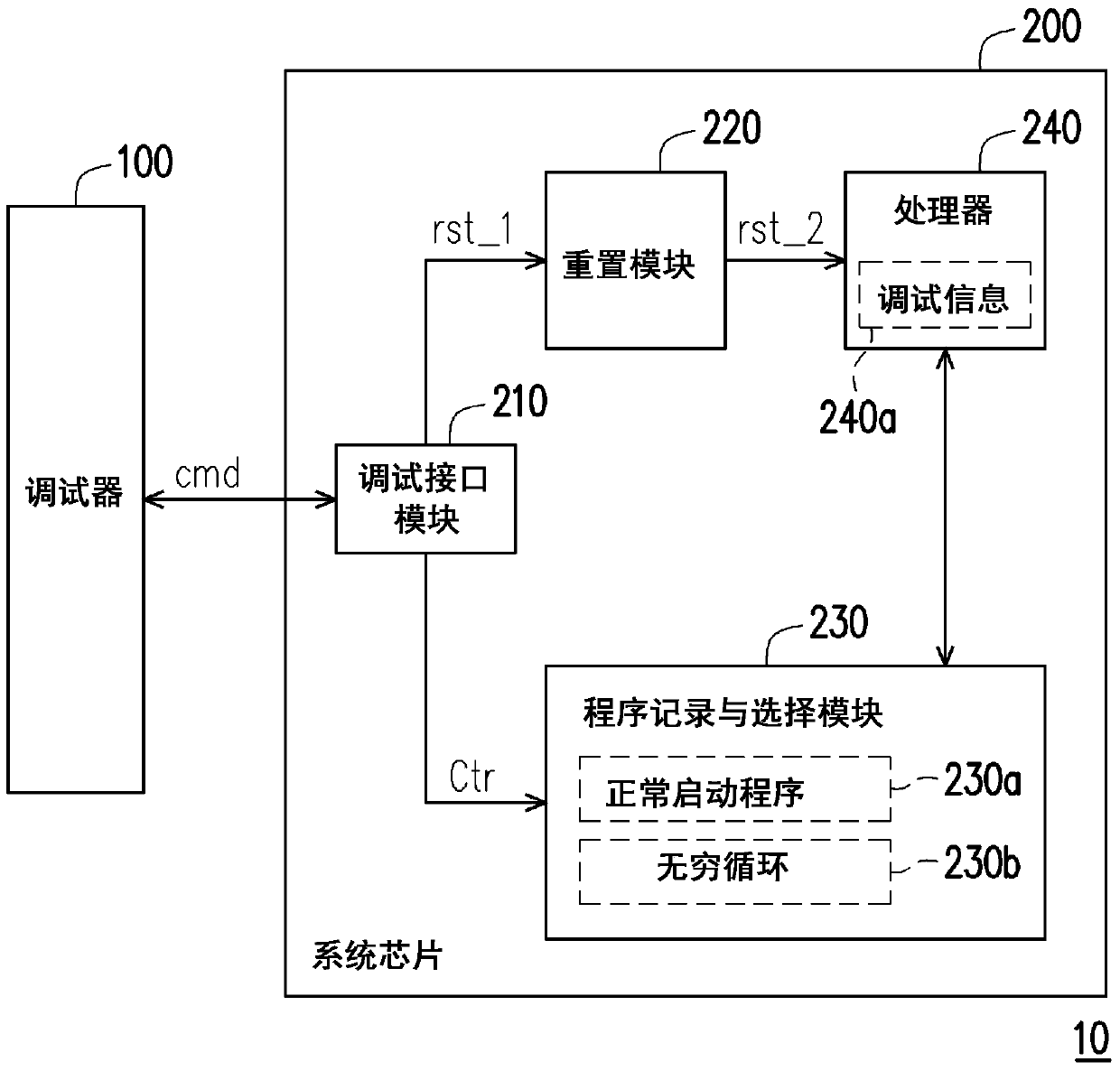
[0045] figure 1 It is a schematic block diagram of a chip debugging system according to an embodiment of the present invention. Please refer to figure 1, the chip debugging system 10 includes a debugger 100 and a system chip 200 . The SoC 100 is formed by constructing many types of circuit modules with different functions on a single chip. For example, the SoC 100 may include elements such as a processor, a digital signal processor, or a memory. The debugger 100 is a computer program and tool for debugging ot...


PUM


Abstract

The invention provides a chip debugging system capable of retaining debugging information. The chip debugging system comprises a debugging device and a system chip. The system chip comprises a debugging interface module, a reset module, a program recording and selection module and a processor, wherein the debugging interface module is connected to the debugging device so as to receive a control command, and a control signal and a reset signal can be generated according to the control command; the reset module is in coupled connection with the debugging interface module, responds to the received reset signal and then generates a system reset signal; the program recording and selection module is in coupled connection to the debugging interface module so as to receive the control signal and adjust a working state of the module according to the control signal; and the processor is in coupled connection to the reset module, responds to the received system reset signal and thus restarts the system, so an infinite cyclic program or a normal start program can be operated according to the working state of the program recording and selection module.

Description

technical field [0001] The present invention relates to a chip debugging system, method and system chip, and in particular to a chip debugging system, method and system chip capable of retaining debugging information. Background technique [0002] With the vigorous development of various electronic products, in the process of R&D and manufacturing of system chips in electronic products, developers must spend more time and manpower on the designed or manufactured system chips to carry out system chip development. Debugging and debugging. Therefore, it has been developed to establish a measurement circuit in the system chip, and replace the probe detection with a small number of test pins and a serial transmission method. At present, this kind of architecture has been established as an industry standard, and it is called JTAG (JointTest Action Group). At present, most SoCs provide JTAG boundary-scan test structure for testing, development and simulation. Generally speaking,...

Claims


Application Information

Patent Timeline
Patent Type & Authority Patents(China)
IPC IPC(8): G06F11/267
CPCG06F11/267
Inventor 温浪明温海华
Owner ALI CORP
Why Eureka
Try Eureka