Supercharge Your Innovation With Domain-Expert AI Agents!

Linear CCD (charge coupled device) signal amplification circuit structure and amplification implementation method thereof

A signal amplifying circuit and signal amplifying technology are applied in the directions of amplification control, negative feedback circuit arrangement, and improving the amplifier to reduce the influence of noise. Stable and reliable effect

Active Publication Date: 2017-05-17
FUJIAN MOREFUN ELECTRONICS TECH CO LTD
View PDF5 Cites 0 Cited by
  • Summary
  • Abstract
  • Description
  • Claims
  • Application Information

AI Technical Summary

Problems solved by technology

[0004] One of the technical problems to be solved by the present invention is to provide a linear CCD signal amplification circuit structure, which has the characteristics of simple circuit, reliable performance and low cost, and can effectively solve the problem of The structure is too complex and the design cost is high

Method used


Image

  • Linear CCD (charge coupled device) signal amplification circuit structure and amplification implementation method thereof

Examples


Embodiment Construction

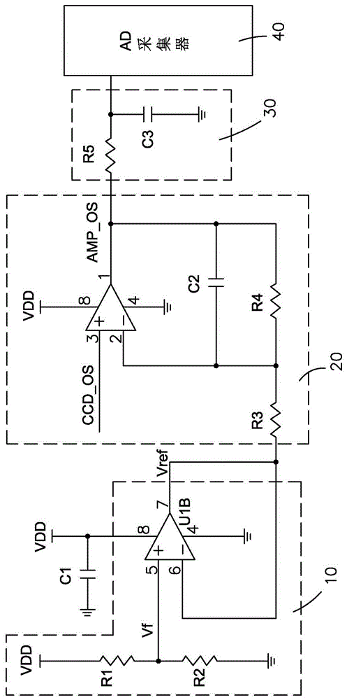
[0017] see figure 1 Shown, a kind of linear CCD signal amplifying circuit structure, described circuit structure comprises DC reference level input circuit 10, CCD signal amplifying circuit 20, filter circuit 30, and AD collector 40; Described DC reference level input circuit 10 , CCD signal amplifying circuit 20, filter circuit 30, and AD collector 40 are connected in sequence; the CCD signal amplifying circuit 20 includes a resistor R3, a resistor R4, a capacitor C2, and an operational amplifier U1A; the DC reference level input circuit 10 and The resistor R3 is connected, the capacitor C2 is connected in parallel with the resistor R4 and then connected in series with the resistor R3; the filter circuit 3 is connected to the first pin of the operational amplifier U1A, and the two ends of the capacitor C2 are respectively connected to the operational amplifier The first pin and the second pin of U1A, the linear CCD output signal CCD_OS is connected to the third pin of the ope...


PUM


Abstract

The invention provides a linear CCD signal amplification circuit structure. The linear CCD signal amplification circuit structure comprise a direct current reference level input circuit, a CCD signal amplification circuit, a filter circuit and an AD (analog / digital) collector which are sequentially connected, wherein the CCD signal amplification circuit is composed of a resistor R3, a resistor R4, a capacitor C2 and operational amplifiers U1A; the direct current reference level input circuit is connected with the resistor R3, the capacitor C2 is connected in parallel with the resistor R4 and then connected in series with the resistor R3; the filter circuit is connected with the first pin of the operational amplifiers U1A; both ends of the capacitor C2 are connected with the first pin and the second pin of the operational amplifiers U1A respectively; linear CCD output signals CCD_OS are connected with the third pin the operational amplifier U1As. The invention also provides a linear CCD signal amplification implementation method. According to the linear CCD signal amplification circuit structure, through treatment on direct current signals and small signals of CCD output signals by two operational amplifiers, post AD data collection can be facilitated, and circuit simplification, performance reliability and low cost can be achieved.

Description

technical field [0001] The invention relates to the technical field of electronic products, in particular to a linear CCD signal amplifying circuit structure and an amplifying realization method thereof. Background technique [0002] CCD is a semiconductor device that converts optical images into digital signals. Its working principle is: the photosensitive element can generate charge when it is exposed to external light, and the charge is stored in the MOS (metal-oxide-semiconductor) unit, and the amount of charge generated is proportional to the intensity of light and the irradiation time. Driven by a sequential external circuit, the charges stored in the CCD can be shifted out sequentially. In the process of CCD application, in addition to the complex driving signal generation circuit, the post-processing of the output analog signal is also very important, which directly affects the image quality. Therefore, the design of the post-stage circuit becomes the key to analog-...

Claims


Application Information

Patent Timeline
Patent Type & Authority Applications(China)
IPC IPC(8): H03F1/26H03F1/34H03G3/20
CPCH03F1/26H03F1/34H03G3/20
Inventor 苏友仲谢纯珀
Owner FUJIAN MOREFUN ELECTRONICS TECH CO LTD
Features
  • R&D
  • Intellectual Property
  • Life Sciences
  • Materials
  • Tech Scout
  • Unparalleled Data Quality
  • Higher Quality Content
  • 60% Fewer Hallucinations
Learn More