
Formation method of test pattern

A technology for testing graphics and graphics, which is applied to the photographic process of patterned surfaces, originals for photomechanical processing, instruments, etc., can solve problems such as product yields that need to be improved, and achieve rich types and quantities and high yields Effect

Active Publication Date: 2020-04-07
SEMICON MFG INT (SHANGHAI) CORP +1
View PDF3 Cites 0 Cited by
  • Summary
  • Abstract
  • Description
  • Claims
  • Application Information

AI Technical Summary

Problems solved by technology

[0005] However, the yield rate of products manufactured by dual patterning technology in the prior art still needs to be improved

Method used


Image

  • Formation method of test pattern
  • Formation method of test pattern
  • Formation method of test pattern

Examples


Embodiment Construction

[0022] As mentioned in the background art, the yield rate of the products manufactured by adopting the dual patterning technology in the prior art still needs to be improved.

[0023] After research, it is found that when the prior art performs various inspections on the first design pattern and the second design pattern obtained by dismantling, it is actually compared with the test pattern in the test pattern library (library), that is to say, the test The type and quantity of test patterns in the pattern library will affect the detection results. For example, the test patterns in the test pattern library have fewer types or fewer quantities. After various tests such as the aforementioned constraint check (Constraint Check), conflict check (Conflict Check), and optical proximity correction check (Optical Printing Check), the obtained In fact, the first design graphic and the second design graphic may not be the optimal dismantling graphic. When the first design graphic and th...


PUM

PropertyMeasurementUnit
lengthaaaaaaaaaa
widthaaaaaaaaaa

Abstract

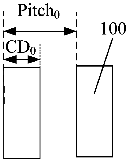
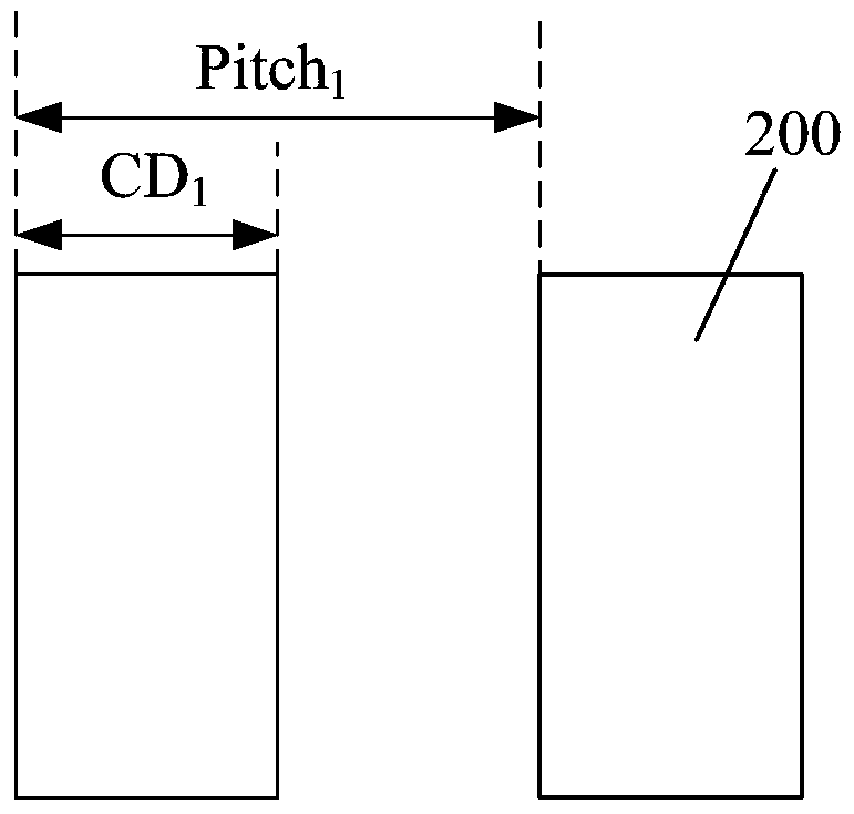
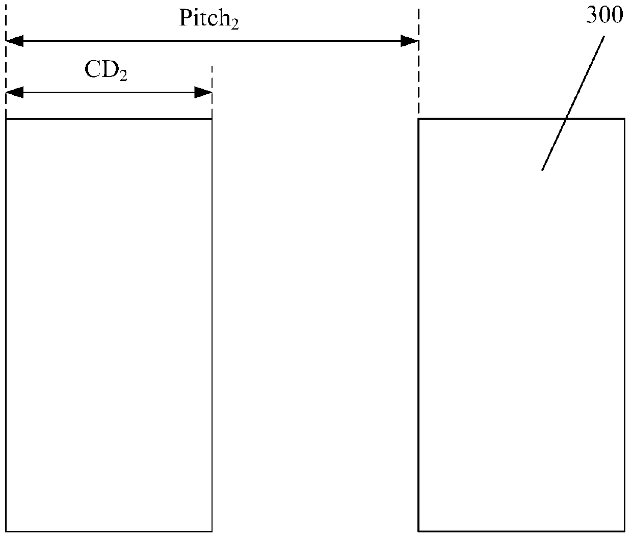
A method for forming test patterns is provided; original test patterns in an original test pattern library are subjected to a series of transformation, and finally, a first test pattern and a second test pattern are obtained; the first test pattern and the second test pattern are added to the original test pattern library, and a new test pattern library is formed. In addition to comprising a plurality of original test patterns, the new test pattern library also comprises the first test pattern and the second test pattern, so the types and number of the test patterns in the new test pattern library are greatly enriched. Therefore, when original design patterns provided by customers are disassembled and detected subsequently, a best and most accurate first design pattern and second design pattern can be obtained, so as to help to form a higher-yield product subsequently.

Description

technical field [0001] The invention relates to the technical field of semiconductor manufacturing, in particular to a method for forming test patterns. Background technique [0002] Semiconductor technology continues to move towards smaller process nodes driven by Moore's Law. With the continuous advancement of semiconductor technology, the functions of devices are becoming more and more powerful, and the difficulty of semiconductor manufacturing is also increasing day by day. Photolithography technology is the most critical production technology in the semiconductor manufacturing process. As the semiconductor process node becomes lower and lower, the minimum line width and spacing designed in semiconductor technology continue to shrink. When the characteristic size of the exposure line is close to the theoretical resolution of the exposure system When the rate limit is reached, the imaging on the surface of the semiconductor substrate will produce serious distortion, whic...

Claims


Application Information

Patent Timeline
Patent Type & Authority Patents(China)
IPC IPC(8): G03F1/44G03F1/36
Inventor 杨青
Owner SEMICON MFG INT (SHANGHAI) CORP
Learn More