Deposition method and sputtering device

A film forming method and sputtering technology, which can be used in sputtering, vacuum evaporation, ion implantation and other directions, and can solve problems such as disturbing film quality.

Active Publication Date: 2017-05-24
NISSIN ELECTRIC CO LTD
View PDF5 Cites 5 Cited by
  • Summary
  • Abstract
  • Description
  • Claims
  • Application Information

AI Technical Summary

Problems solved by technology

[0004] Its reason is: in existing general magnetron sputtering method, refer to figure 1 Plasma is generated by applying high-frequency or DC target power to the target, and the target is sputtered using the target power to form a film on the subst

Method used


Image

  • Deposition method and sputtering device
  • Deposition method and sputtering device
  • Deposition method and sputtering device

Examples


Embodiment Construction

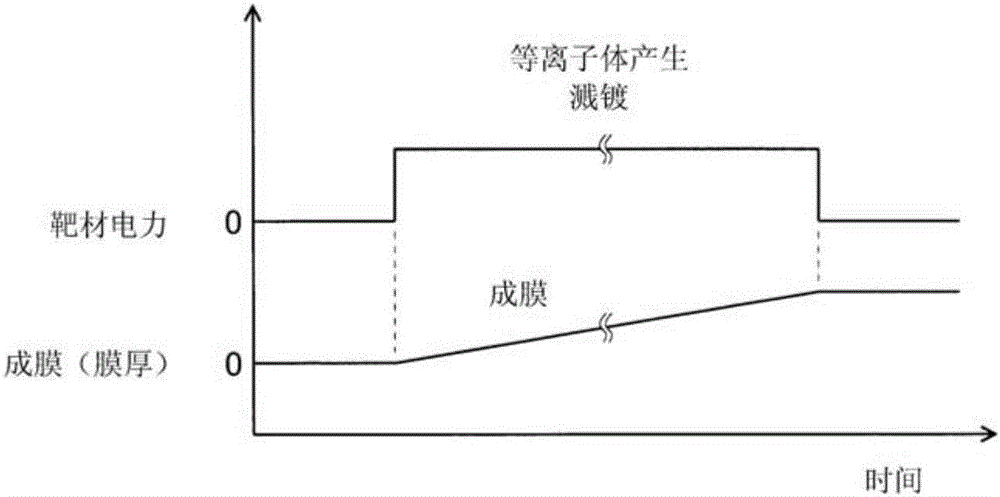
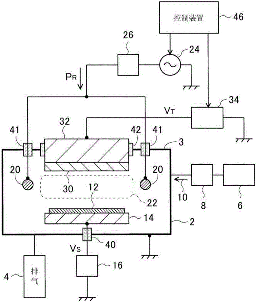
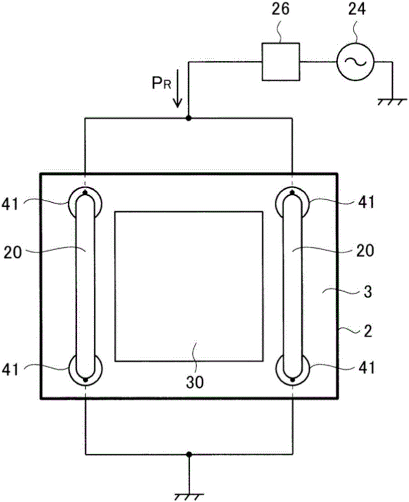
[0029] An example of a sputtering device for implementing the film forming method of the present invention is shown in figure 2 , will be observed from below figure 2 A diagram around the antenna of the device shown in the image 3 middle. exist figure 2 , conceptually represents the high-frequency power P for each antenna 20 R The power supply section, regarding the power supply section, will refer to image 3 And later.

[0030] The sputtering device includes a vacuum container 2 that is evacuated by a vacuum exhaust device 4, and the vacuum container 2 is electrically connected to the ground.

[0031] A sputtering gas 10 is introduced into the vacuum vessel 2 . In the above example, the gas is introduced from the gas source 6 through the flow regulator 8 . The gas 10 is, for example, argon. When reactive sputtering is performed, the gas 10 may be a mixed gas of argon and active gas (such as oxygen, nitrogen, etc.).

[0032] A substrate holder 14 holding a substr...


PUM


Abstract

The purpose of the present invention is to prevent deposition of an uneven film at the start or end of film deposition without having to install a movement mechanism for a target. This sputtering device generates inductively coupled plasma (22) by supplying high-frequency power (PR) to an antenna (20) provided in a vacuum vessel (2) into which a gas (10) is introduced, and uses the plasma (22) and a target bias voltage (VT) to sputter a target (30) and deposit a film on a substrate (12). At the start of film deposition, the target bias voltage (VT) is applied to the target (30) to initiate sputtering after the high-frequency power (PR) has been supplied to the antenna (20) and the plasma (22) has been generated, and at the end of film deposition, the target bias voltage (VT) applied to the target (30) is stopped to stop sputtering, after which the high-frequency power (PR) supplied to the antenna (20) is stopped to quench the plasma (22).

Description

technical field [0001] The present invention relates to a film forming method and a sputtering device for forming a film on a substrate by sputtering (in other words, film formation; the same applies hereinafter). More specifically, the present invention relates to a method for supplying high frequency power to an antenna to A film forming method and a sputtering device for sputtering a target by generating inductively coupled plasma (abbreviated as ICP). Background technique [0002] As materials for thin-film transistors (TFTs) for high-precision displays, for example, IGZO (In-Ga-Zn-O / Indium-Gallium-Zinc-Oxygen), ITZO (In-Sn-Zn-O / Indium-Tin-Zinc Oxide semiconductors such as -oxygen) have attracted attention. [0003] In many cases, such thin films of oxide semiconductors for TFTs are formed by magnetron sputtering (magnetronsputtering) method that utilizes electric and magnetic fields to perform magnetron The electrons can move along a continuous trajectory near the tar...

Claims


Application Information

Patent Timeline
IPC IPC(8): C23C14/34H01L21/363H05H1/46
CPCC23C14/34H05H1/46C23C14/3471H01J37/3408H01J37/3444
Inventor 瀬戸口佳孝岸田茂明安东靖典
Owner NISSIN ELECTRIC CO LTD
Why Eureka
Try Eureka