Three-dimensional device and manufacturing method thereof
A technology for a stereoscopic display device and a display unit, applied in optics, instruments, nonlinear optics, etc., can solve problems such as crosstalk, unsatisfactory effects, and increased user discomfort.
- Summary
- Abstract
- Description
- Claims
- Application Information
AI Technical Summary
Problems solved by technology
Method used
Image
Examples
no. 1 example
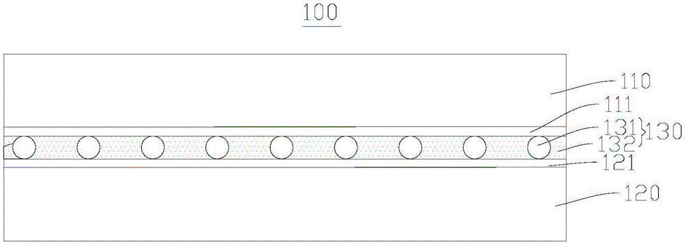
[0034]The first embodiment of the present invention provides a stereoscopic display device 100, please refer to image 3 , the stereoscopic display device 100 includes: a 2D display unit 110 and a 3D functional device 120 , the 2D display unit 110 and the 3D functional device 120 are disposed opposite to each other. The first substrate 111 of the 2D display unit 110 is fixedly connected to the second substrate 121 of the 3D functional device 120 through the adhesive layer 130 .
[0035] The 2D display unit 110 may be, for example, a liquid crystal display unit, please refer to Figure 4 , including a backlight unit 117 and a display panel 112 . Wherein, the backlight unit 117 may be a direct type or an edge type backlight unit 117 including LED (Led Emitting Diode) or CCFL (Cold Cathode Fluorescent Lamp) and other light sources. The display panel 112 may be a TFT_LCD (Thin Film Transistor-Liquid Crystal Display), or other 2D display units 110 . Of course, when the 2D displa...
no. 2 example
[0049] The second embodiment of the present invention provides a method for manufacturing a stereoscopic display device, please refer to Figure 7 , the manufacturing method of the stereoscopic display device comprises:
[0050] Step S110: Coating an adhesive material on the surface of the first substrate of the 2D display unit or the second substrate of the 3D functional device, the adhesive material including adhesive glue and spacers.
[0051] The spacer is an object of uniform size, the spacer is in a transparent state, and the surface of the spacer includes a plurality of small holes. Or the spacer is a rod-shaped object with a round cross section, the spacer is in a transparent state, and the surface of the spacer includes a plurality of small holes.
[0052] Specifically, step S110 may be: coating adhesive on the surface of the first substrate of the 2D display unit or the second substrate of the 3D functional device; and uniformly dispersing spacers in the coated adhe...
PUM
 Abstract
Description
Claims
Application Information
 - R&D
- Intellectual Property
- Life Sciences
- Materials
- Tech Scout
- Unparalleled Data Quality
- Higher Quality Content
- 60% Fewer Hallucinations
Browse by: Latest US Patents, China's latest patents, Technical Efficacy Thesaurus, Application Domain, Technology Topic, Popular Technical Reports.
© 2025 PatSnap. All rights reserved.Legal|Privacy policy|Modern Slavery Act Transparency Statement|Sitemap|About US| Contact US: help@patsnap.com


