Liquid crystal panel and liquid crystal display

A liquid crystal panel and substrate technology, which is applied in the direction of instruments, nonlinear optics, optics, etc., can solve the problems of thin film transistor electrical curve drift and so on

Inactive Publication Date: 2017-05-31
WUHAN CHINA STAR OPTOELECTRONICS TECH CO LTD
View PDF8 Cites 2 Cited by
  • Summary
  • Abstract
  • Description
  • Claims
  • Application Information

AI Technical Summary

Problems solved by technology

[0004] At present, the black matrix (BM) set on the CF substrate corresponds to the thin film transistor set on the Array substrate, so that the black matrix can effectively block the light in the environment from illuminating the active layer of the thin film transistor, but the light passes through the diffraction and liquid crystal. Reflection and other methods will still irradiate the active layer of the thin film transistor, which will cause the electrical curve of the thin film transistor to drift

Method used


Image

  • Liquid crystal panel and liquid crystal display
  • Liquid crystal panel and liquid crystal display
  • Liquid crystal panel and liquid crystal display

Examples


Embodiment Construction

[0020] Hereinafter, embodiments of the present invention will be described in detail with reference to the accompanying drawings. This invention may, however, be embodied in many different forms and should not be construed as limited to the specific embodiments set forth herein. Rather, the embodiments are provided to explain the principles of the invention and its practical application, thereby enabling others skilled in the art to understand the invention for various embodiments and with various modifications as are suited to particular intended uses.

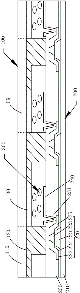
[0021] In the drawings, the thicknesses of layers and regions are exaggerated for device clarity. It will be understood that when an element is referred to as being "disposed on" or "on" another element, it can be directly on the other element or intervening elements may also be present.

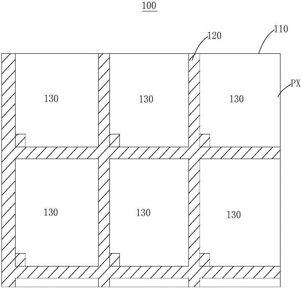
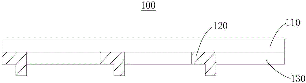
[0022] figure 1 is a top view of the color filter substrate according to the first embodiment of the present invention. figure 2 Yes ...


PUM


Abstract

The invention discloses a liquid crystal panel. The liquid crystal panel comprises an array substrate and a color film substrate, wherein the array substrate comprises a first substrate and a plurality of thin film transistors arranged on the first substrate in an array form; the color film substrate and the array substrate are arranged in a cassette-to-cassette form; the color film substrate comprises a second substrate and black matrixes arranged on the second substrate; part or all of the black matrix opposite to the thin film transistors extend to prop against the array substrate. According to the liquid crystal panel disclosed by the invention, all the black matrixes of the color film substrate or parts, opposite to the thin film transistors, of the black matrixes extend and are protruded, so as to make propping contact with an insulated protecting layer of the array substrate, further light formed by modes such as diffraction or liquid crystal reflection is prevented from irradiating on semiconductor layers of the thin film transistors, and eventually, electrical curve drift of the thin film transistors is avoided.

Description

technical field [0001] The invention belongs to the technical field of liquid crystal display, and in particular relates to a liquid crystal panel and a liquid crystal display. Background technique [0002] With the evolution of optoelectronics and semiconductor technology, it has also led to the vigorous development of flat panel displays. Among many flat panel displays, liquid crystal displays (LCD for short) have high space utilization efficiency and low power consumption. , no radiation and low electromagnetic interference and many other superior characteristics have been applied in all aspects of production and life. [0003] The liquid crystal display is generally a backlight type liquid crystal display, which includes a liquid crystal panel and a backlight module disposed opposite to each other. The working principle of the liquid crystal panel is to place liquid crystal molecules in two parallel glass substrates (that is, the color filter substrate (CF substrate) an...

Claims


Application Information

Patent Timeline
Patent Type & Authority Applications(China)
IPC IPC(8): G02F1/1335
Inventor 余威
Owner WUHAN CHINA STAR OPTOELECTRONICS TECH CO LTD
Why Eureka
Try Eureka