Neural network space mapping modeling method for packaged transistors

A neural network and modeling method technology, applied in the field of microwave circuit and device modeling, can solve problems such as the inability to reflect the impact of packaged circuits on transistor performance, and achieve the effect of accurate reflection and simple neural network structure

Inactive Publication Date: 2017-05-31
TIANJIN POLYTECHNIC UNIV +1
View PDF0 Cites 5 Cited by
  • Summary
  • Abstract
  • Description
  • Claims
  • Application Information

AI Technical Summary

Problems solved by technology

However, the existing neural network space mapping modeling method is mainly aimed at the modeling of the transi

Method used


Image

  • Neural network space mapping modeling method for packaged transistors
  • Neural network space mapping modeling method for packaged transistors
  • Neural network space mapping modeling method for packaged transistors

Examples


Embodiment Construction

[0033] In order to make the object, technical solution and advantages of the present invention clearer, the embodiments of the present invention will be described in detail below with reference to the accompanying drawings.

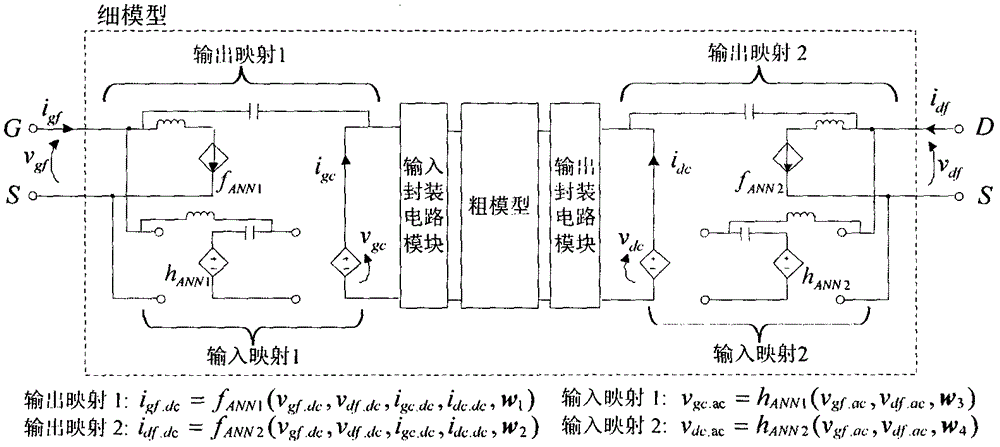
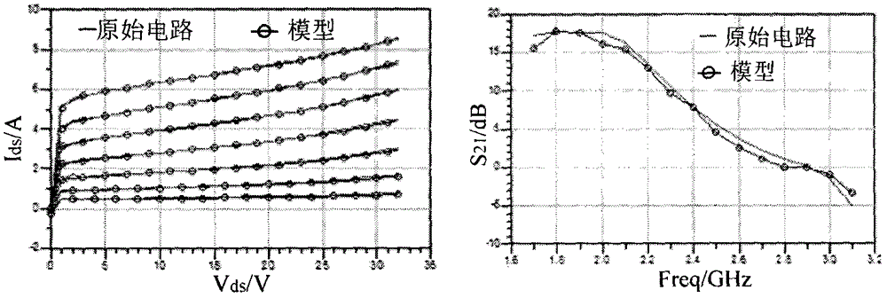
[0034] When adopting the modeling method proposed by the present invention to model the packaged transistor, its model structure is as follows figure 1 shown. The model is mainly divided into four parts: the input package circuit module, the rough model module, the output package circuit module and the mapping circuit. Simulate the non-linear characteristics of packaged transistor dies, using mapping circuits to tune the characteristics of the entire model.

[0035] The existing model is selected as the rough model module of the package transistor model. If the transistor model researched by the device manufacturer is selected as the rough model, its performance should be as close as possible to the performance of the packaged transistor being modeled; ...


PUM


Abstract

The invention provides a neural network space mapping modeling method for packaged transistors. Building of accurate packaged transistor models is of vital importance on improving the precision of wireless communication system circuits. The neural network space mapping modeling method aims to overcome the shortcomings of requirements on internal structure information and high computational complexity of existing modeling methods for packaged transistors. The neural network space mapping modeling method for the packaged transistors includes dividing each packaged transistor model into an input packaged circuit module, a nonlinear circuit module and an output packaged circuit module; respectively constructing structures of the input packaged circuit modules, the nonlinear circuit modules and the output packaged circuit modules. The neural network space mapping modeling method has the advantages that characteristics of the packaged transistors can be accurately reflected by trained models, the neural network space mapping modeling method is high in simulation speed, the design cycle can be greatly shortened, and large-scale circuits can be possibly further designed.

Description

technical field [0001] The invention relates to a microwave circuit and device modeling method, in particular to the application of neural network space mapping technology in the field of microwave modeling. Background technique [0002] In order to meet the development requirements of low cost, low power consumption, high precision, high reliability, and intelligent electronic products, the structure of power transistors used in wireless communication systems is becoming more and more complex. In addition to adding multiple dies to provide power, transistors Bonding wires and MOS capacitors in internal package circuits are also increased to ensure transistor stability and performance. The coupling between the components inside the transistor and the parasitic effects of the packaging circuit should have an increasing impact on the performance of the transistor, which poses a huge challenge to the CAD modeling technology. [0003] At present, there are two main modeling met...

Claims


Application Information

Patent Timeline
IPC IPC(8): G06F17/50
CPCG06F30/30
Inventor 闫淑霞靳晓怡赵宝柱赵靖曹宇
Owner TIANJIN POLYTECHNIC UNIV
Why Eureka
Try Eureka