Display panel detecting device and display panel detecting method

A technology of display panel and detection device, which is applied in static indicators, image data processing, instruments, etc., and can solve problems such as inability to detect

Active Publication Date: 2017-05-31
BOE TECH GRP CO LTD +1
View PDF10 Cites 8 Cited by
  • Summary
  • Abstract
  • Description
  • Claims
  • Application Information

AI Technical Summary

Problems solved by technology

For tiny shells (shells refer to non-penetrating surface damage, similar in shape to shells) or damage in the edge electrode area of ​​the flat panel display

Method used


Image

  • Display panel detecting device and display panel detecting method
  • Display panel detecting device and display panel detecting method
  • Display panel detecting device and display panel detecting method

Examples


Embodiment 1

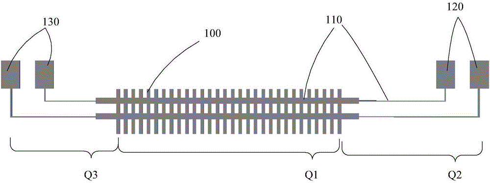
[0039] Figure 4 It is a schematic diagram of the display panel detection device of the first embodiment, as Figure 4 As shown, in the display panel detection device of this embodiment: a plurality of data lines 100 are arranged on the electrode area Q1, and two short-circuit bars 110 are intersected on the data lines 100. For example, the data lines 100 can be divided into odd-numbered rows and The even-numbered rows are divided into two groups, and each short-circuit bar 110 is used to short-circuit a group of data lines 100 together. The short-circuit bars 110 extend from both sides to the first detection area Q2 and the second detection area on both sides of the electrode area Q1. In area Q3, both ends of each short-circuit bar 110 are respectively connected to the first pad 120 and the second pad 130 . Of course, the grouping method of the data lines 100 is not limited to the above-mentioned method, and other grouping methods can also be adopted without departing from t...

Embodiment 2

[0055] In this embodiment, the switch 200 is a field effect transistor, which has the advantages of fast response, small leakage and high power.

[0056] In this embodiment, all the short-circuit bars 110 on one side are disconnected from the short-circuit bar signal input pads 120, and connected by field effect transistors, the drains of the field effect transistors are connected to the short-circuit bars 110, and the sources are connected to the short-circuit bars The signal input pad 120; the electrodes of the field effect transistors are shorted together and connected to the switch signal input Pad. The trimming process of the FET and signal input pad after the panel function test will be cut by laser, which will not affect the subsequent MDL (Module, module process (adding backlight, PCB, shell, etc. results)) process.

[0057] In this embodiment, the switch signal for controlling the input of the single-side short-circuit bar signal is added. When the switch signal is in...

Embodiment 3

[0060] Compared with the first embodiment, the detection structure of the display panel in this embodiment further includes: a redundant first pad 121 with the same size as the first pad 120 and arranged on the same side, and a redundant first pad 121 with the second pad 120 130 is a redundant second pad 131 with the same size and arranged on the same side; wherein, the first pad 120 and the redundant first pad 121 are located at the positions of the second pad 130 and the redundant second pad 131 symmetrical settings such as Figure 8 shown.

[0061] The reason why the redundant first pad 121 and the redundant second pad 131 are set is that the detection probe module 150 for detecting the data lines 100 of different types of display panels can be used in common, and for different types of display panel design The relative positions of all the first pads 120 and the second pads 130 are the same. When detecting signals, the detection probe 140 is suspended in the non-signal p...


PUM


Abstract

The invention provides a display panel detecting device. The device is used for detecting signal lines on a display panel. The signal lines at least comprise multiple data lines, and the data lines are divided into N groups. The display panel detecting device comprises N short-circuiting stripes in a electrode zone of the display panel and a plurality of bonding pads, the bonding pads are arranged on the two sides of the electrode zone, each short-circuiting stripe is used for making a group of the data lines in short connection together, the two ends of each short-circuiting stripe are each connected with one bonding pad, the bonding pads are arranged on the same side of all the short-circuiting stripes, and one switch is arranged between each short-circuiting stripe and the corresponding bonding pads connected with the short-circuiting stripe. The invention further provides a display panel detecting method, by means of the method, the damage location and the damage degree of the polar zone of the display panel can be accurately detected.

Description

technical field [0001] The present invention relates to but not limited to the field of display technology, and in particular relates to a display panel inspection device and a display panel inspection method. Background technique [0002] Liquid Crystal Display (LCD for short) is a flat and ultra-thin display device, which consists of a certain number of color or black and white pixels, and is placed in front of a light source or a reflective surface. Liquid crystal displays have low power consumption, high image quality, small size, and light weight, so they are favored by everyone and become the mainstream of displays. At present, liquid crystal displays are mainly thin film transistor (Thin Film Transistor, TFT for short) liquid crystal displays. [0003] The preparation of the display panel includes the array (Array) substrate process, the color filter (CF) substrate process, and the cell process of the array substrate and the color filter substrate. Generally, the pan...

Claims


Application Information

Patent Timeline
IPC IPC(8): G09G3/00
CPCG09G3/006G06T7/0008G06T2207/10024G06T2207/10152G09G2310/0232G09G2300/0404G06T7/0004G06T2207/30121G06T7/90
Inventor 历伟马明辉曹金虎曹斌权南仁于嘉鑫于凤武高棉
Owner BOE TECH GRP CO LTD
Why Eureka
Try Eureka