An electrostatic protection circuit, an array substrate, a display panel, and a display device

A static protection, array substrate technology, applied in the direction of circuits, electrical components, electrical solid devices, etc., can solve the problems of less paths, poor static effect, etc., and achieve the effect of improving the ability of static electricity

Active Publication Date: 2019-05-17
BOE TECH GRP CO LTD +1
View PDF4 Cites 0 Cited by
  • Summary
  • Abstract
  • Description
  • Claims
  • Application Information

AI Technical Summary

Problems solved by technology

In fact, most static electricity can be passed as figure 1 The path ① shown is conducted away, however, some static electricity will still pass through such as figure 1 The path ② shown leads to the inside of the display panel. It can be seen that the existing electrostatic protection circuit has fewer paths to export static electricity, and the effect of static electricity export is not good.

Method used


Image

  • An electrostatic protection circuit, an array substrate, a display panel, and a display device
  • An electrostatic protection circuit, an array substrate, a display panel, and a display device
  • An electrostatic protection circuit, an array substrate, a display panel, and a display device

Examples


example 1

[0062] Example 1: The above electrostatic protection circuit provided by the embodiment of the present invention is applied to an array substrate of a thin film transistor with a top-gate structure, and the active layer, gate, and source (drain) of the thin film transistor are sequentially stacked on the array substrate superior.

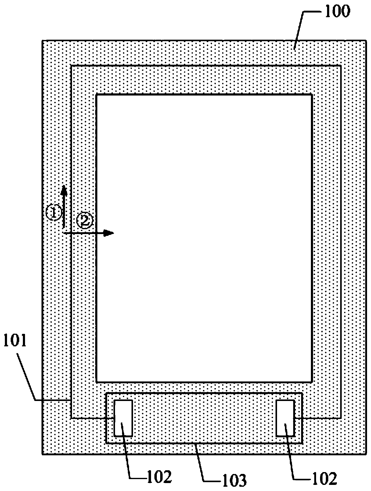
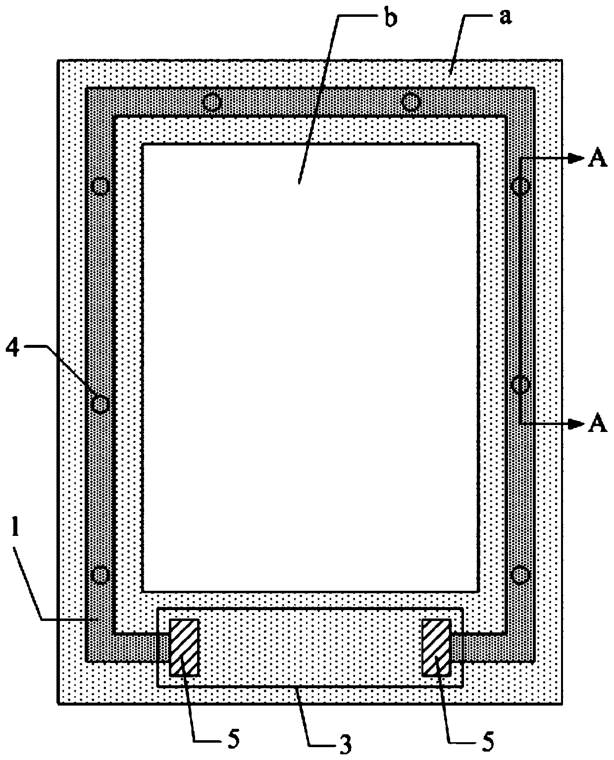
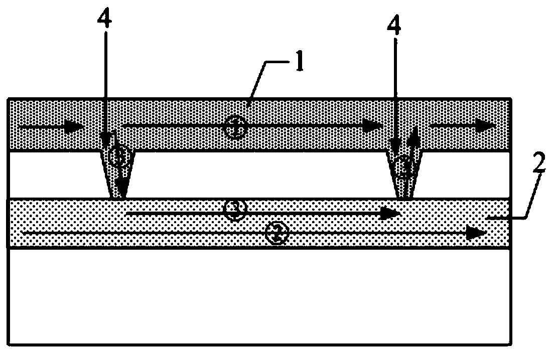
[0063] In specific implementation, in the above-mentioned electrostatic protection circuit provided by the embodiment of the present invention, such as Figure 3a-Figure 3c as shown, Figure 3b for Figure 3a Sectional view along B1B1 direction, Figure 3c for Figure 3a A cross-sectional view along the B2B2 direction, the third ground line 6, the second ground line 2 and the first ground line 1 are sequentially stacked on the array substrate; as Figure 3b As shown, the second ground wire 2 has a third via hole 8 that runs through the film layer where the second ground wire 2 is located and has a diameter larger than that of the second via hole...

example 2

[0068]Example 2: The above electrostatic protection circuit provided by the embodiment of the present invention is applied to an array substrate of a thin film transistor with a top-gate structure, and the source (drain), active layer, and gate of the thin film transistor are sequentially stacked on the array substrate superior.

[0069] In specific implementation, the above-mentioned electrostatic protection circuit provided by the embodiment of the present invention, such as Figure 5a-5c as shown, Figure 5b for Figure 5a Sectional view along D1D1 direction, Figure 5c for Figure 5a In the cross-sectional view along the direction D2D2, the first ground wire 1, the third ground wire 6 and the second ground wire 2 are sequentially stacked on the array substrate; the above-mentioned electrostatic protection circuit provided by the embodiment of the present invention is as follows Figure 5b and Figure 5c As shown, it may also include: a fourth insulating layer 14 locat...

example 3

[0071] Example 3: The above electrostatic protection circuit provided by the embodiment of the present invention is applied to an array substrate of a thin film transistor with a bottom gate structure, and the gate, active layer, and source (drain) of the thin film transistor are sequentially stacked on the array substrate .

[0072] In specific implementation, in the above-mentioned electrostatic protection circuit provided by the embodiment of the present invention, such as Figure 6a-Figure 6c as shown, Figure 6b for Figure 6a Sectional view along E1E1 direction, Figure 6c for Figure 6a In the cross-sectional view along the E2E2 direction, the second ground line 2, the third ground line 6 and the first ground line 1 are sequentially stacked on the array substrate; Figure 6b and Figure 6c As shown, it may also include: a sixth insulating layer 16 located between the film layer where the first ground line 1 is located and the film layer where the third ground line ...


PUM


Abstract

An electrostatic protection circuit, an array substrate, a display panel and a display device are disclosed. The electrostatic protection circuit is located within a peripheral region of an array substrate and includes: a first ground wire provided in a same layer as a source electrode and a drain electrode of a thin film transistor located within a display region of the array substrate; and a second ground wire provided in a same layer as a gate electrode of the thin film transistor, wherein, the first ground wire forms a first loop with a printed circuit board provided within the peripheral region, the first loop surrounds the display region; the second ground wire forms a second loop with the printed circuit board, and the second loop surrounds the display region.

Description

technical field [0001] The invention relates to the field of display technology, in particular to an electrostatic protection circuit, an array substrate, a display panel and a display device. Background technique [0002] During the manufacturing process of the display panel, static electricity may be generated in many processes. If static electricity is introduced into the array substrate, it will cause abnormal display of the display panel during the static electricity test, and, for the structure of the gate drive circuit integrated in the array substrate (Gate On Array, GOA), the static electricity will also affect the GOA circuit. If static electricity is introduced into the color film substrate, it will cause the display panel to appear red; therefore, in order to avoid static electricity from damaging the display panel, an electrostatic protection circuit is generally installed in the display panel. [0003] Existing ESD protection circuits such as figure 1 As show...

Claims


Application Information

Patent Timeline
Patent Type & Authority Patents(China)
IPC IPC(8): H01L27/02H01L27/12H01L23/60
CPCH01L23/60H01L27/0248H01L27/1214G02F1/136204G02F2202/22H01L27/0288H01L27/0292H01L27/0296H01L27/124H01L23/5226H01L23/528H01L23/53271
Inventor 任艳伟徐敬义张琨鹏刘宇刘敏田瑞英
Owner BOE TECH GRP CO LTD
Why Eureka
Try Eureka