
Manufacturing method for shallow trench isolation floating gate structure and manufacturing method for floating gate type flash memory

A fabrication method and shallow trench technology, which are applied to electrical components, electrical solid-state devices, circuits, etc., can solve the problems of many polysilicon residues, complicated processes, surface depressions of electronic storage layers, etc., and achieve the effect of low cost and simple process.

Inactive Publication Date: 2017-05-31
WUHAN XINXIN SEMICON MFG CO LTD
View PDF5 Cites 1 Cited by
  • Summary
  • Abstract
  • Description
  • Claims
  • Application Information

AI Technical Summary

Problems solved by technology

[0014] The purpose of the present invention is to solve the problem that the traditional manufacturing method of shallow trench isolation floating gate structure is complicated
[0015] Another object of the present invention is to solve the problems of the electron storage layer surface depression and polysilicon residues

Method used


Image

  • Manufacturing method for shallow trench isolation floating gate structure and manufacturing method for floating gate type flash memory
  • Manufacturing method for shallow trench isolation floating gate structure and manufacturing method for floating gate type flash memory
  • Manufacturing method for shallow trench isolation floating gate structure and manufacturing method for floating gate type flash memory

Examples


Embodiment Construction

[0041] The manufacturing method of the shallow trench isolation floating gate structure and the manufacturing method of the floating gate flash memory proposed by the present invention will be further described in detail below with reference to the accompanying drawings and specific embodiments. Advantages and features of the present invention will be apparent from the following description and claims. It should be noted that all the drawings are in a very simplified form and use imprecise scales, and are only used to facilitate and clearly assist the purpose of illustrating the embodiments of the present invention.

[0042] Such as Figure 10 As shown, an embodiment of the present invention provides a method for manufacturing a shallow trench isolation floating gate structure, including the following steps:

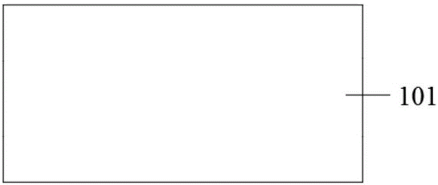
[0043] S1. Provide a semiconductor substrate;

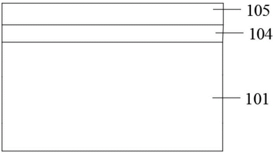
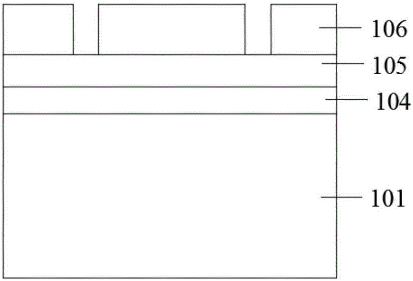
[0044] S2, sequentially forming an electron channel layer and an electron storage layer on the semiconductor substrate;...


PUM


Abstract

The invention provides a manufacturing method for a shallow trench isolation floating gate structure and a manufacturing method for a floating gate type flash memory. The manufacturing method for the shallow trench isolation floating gate structure comprises the steps of providing a semiconductor substrate; forming an electronic channel layer and an electronic storage layer on the semiconductor substrate in sequence; forming a patterned photoresist layer on the electronic storage layer; taking the patterned photoresist layer as a mask, etching the electronic storage layer, the electronic channel layer and a part of the semiconductor substrate to form a plurality of trenches, and then removing the patterned photoresist layer; filling the trenches with an insulating material, wherein the insulating material covers the electronic storage layer; and adopting a chemical grinding process to remove the insulating material on the electronic storage layer to form the shallow trench isolation floating gate structure. The process is simple and the cost is relatively low; and meanwhile, the problem of pits generated in the surface of the electronic storage layer in the grinding process can be avoided, and the yield of a semiconductor device can be improved.

Description

technical field [0001] The invention relates to the technical field of integrated circuit manufacturing, in particular to a manufacturing method of a shallow trench isolation (shallow trench isolation) floating gate (Floating Gate) structure and a manufacturing method of a floating gate flash memory. Background technique [0002] Since the shallow trench isolation floating gate structure can increase the contact area between the floating gate and the oxide-nitride-oxide (Oxide-Nitride-Oxide) structure in the subsequent process, and improve the coupling rate of the device, it is used in the floating gate flash memory Shallow trench isolation floating gate structures are often used in the fabrication of chips. [0003] The fabrication method of traditional shallow trench isolation floating gate structure comprises the following steps: [0004] Such as figure 1 As shown, a semiconductor substrate 101 is provided; [0005] Such as figure 2 As shown, an electron channel laye...

Claims


Application Information

Patent Timeline
IPC IPC(8): H01L27/115H01L29/423
CPCH01L29/42324H01L29/42336H10B41/00H10B41/20
Inventor 姚兰周俊
Owner WUHAN XINXIN SEMICON MFG CO LTD
Features
  • Generate Ideas
  • Intellectual Property
  • Life Sciences
  • Materials
  • Tech Scout
  • Unparalleled Data Quality
  • Higher Quality Content
  • 60% Fewer Hallucinations
Learn More