

Silicon-based tunable laser based on mode converter and implementation method thereof
A technology for tunable lasers and mode conversion, applied in lasers, laser parts, semiconductor lasers, etc., can solve the problems of high process complexity and high cost of silicon-based tunable lasers, and achieve reduced process costs, high stability, and reduced complexity. degree of effect
Active Publication Date: 2017-05-31
WUHAN POST & TELECOMM RES INST CO LTD
View PDF4 Cites 2 Cited by
- Summary
- Abstract
- Description
- Claims
- Application Information
AI Technical Summary
Problems solved by technology
[0004] The technical problem to be solved by the present invention is to solve the problems of high process complexity and high cost of existing silicon-based tunable lasers
Method used
View moreImage
Smart ImageViewing Examples

Examples
Embodiment Construction
[0024] The present invention will be described in detail below in conjunction with the accompanying drawings and specific embodiments.
Login to View More PUM
 Abstract
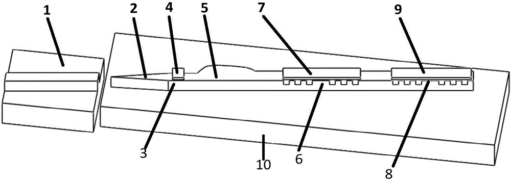
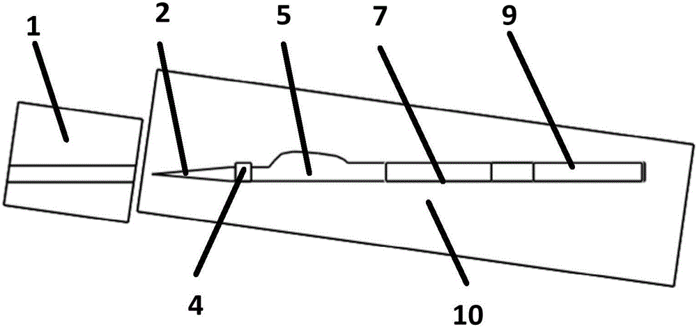
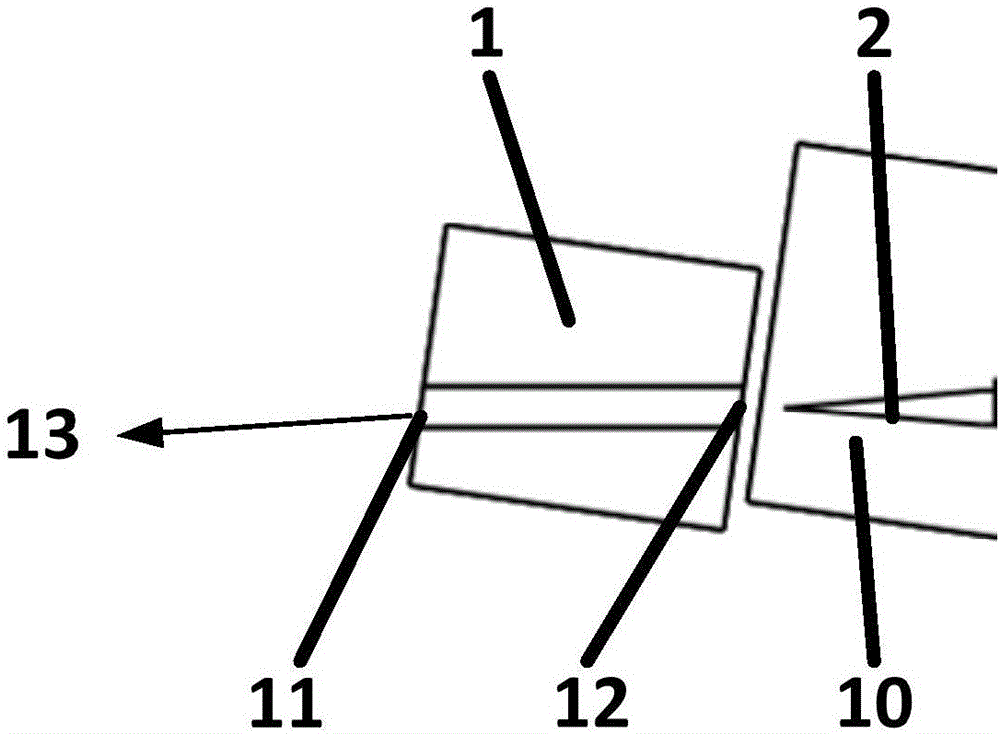
The invention discloses a silicon-based tunable laser based on a mode converter and an implementation method thereof. The silicon-based tunable laser comprises a semiconductor amplifier, a silicon-on-insulator (SOI) wafer, a coupler, a TE0 mode waveguide, the mode converter, a first sampling optical grating and a second sampling optical grating, wherein the coupler, the TE0 mode waveguide, the mode converter, the first sampling optical grating and the second sampling optical grating are sequentially connected with the SOI wafer, the first sampling optical grating and the second sampling optical grating are connected at intervals, the coupler is used for transmitting an optical field output from the semiconductor amplifier to the TE0 mode waveguide to obtain a TE0 mode optical field, the mode converter is used for converting the TE0 mode optical field to a new mode optical field with effective refractive index smaller than that of a TE0 mode, and the first sampling optical grating and the second sampling optical grating are used for reflecting the new mode optical field to the semiconductor amplifier. By the silicon-based tunable laser, more precision processing means is not needed, the process cost is greatly reduced, and the process stability is higher; and meanwhile, the first sampling optical grating and the second sampling optical grating are arranged on the same waveguide, an optical divider can be omitted, and the complexity is reduced.
Description
technical field [0001] The invention relates to the field of optical communication integrated devices, in particular to a silicon-based tunable laser based on a mode converter and a realization method thereof. Background technique [0002] Tunable lasers are important devices in optical communication systems. Traditional tunable lasers are mainly based on micromechanical rotating mirrors and diffraction gratings, which are large in size and not suitable for integration. Silicon-based photonic integration technology is a new technology that has emerged in recent years. It has the advantages of compatibility with semiconductor processes, low cost, and high integration. It is widely used in the integration of tunable lasers to form silicon-based tunable lasers. [0003] At present, silicon-based tunable lasers are mainly realized by microrings with poor process stability. Although the stability of silicon-based reflection gratings is higher than that of microrings, the effectiv...
Claims
Login to View More Application Information
Patent Timeline
 Patent Type & AuthorityApplications(China)
IPC IPC(8): H01S5/065
CPCH01S5/0651
Inventor王磊肖希陈代高李淼峰杨奇余少华
OwnerWUHAN POST & TELECOMM RES INST CO LTD