Flexible printed circuit board and manufacturing method thereof

A technology of flexible circuit boards and manufacturing methods, which is applied in the fields of flexible printed circuit boards, printed circuit manufacturing, multilayer circuit manufacturing, etc., can solve the problems of single-sided contact and conduction of pads, and achieve the goal of reducing pad tearing risk effect

Active Publication Date: 2017-05-31
VIVO MOBILE COMM CO LTD
View PDF4 Cites 3 Cited by
  • Summary
  • Abstract
  • Description
  • Claims
  • Application Information

AI Technical Summary

Problems solved by technology

[0005] The invention provides a flexible circuit board and its manufacturing method to solve the problem that the pads of the existing flexible double-sided board can only be contacted and conducted on one side

Method used


Image

  • Flexible printed circuit board and manufacturing method thereof
  • Flexible printed circuit board and manufacturing method thereof
  • Flexible printed circuit board and manufacturing method thereof

Examples


Embodiment 1

[0034] A method for manufacturing a flexible circuit board provided by an embodiment of the present invention is introduced in detail.

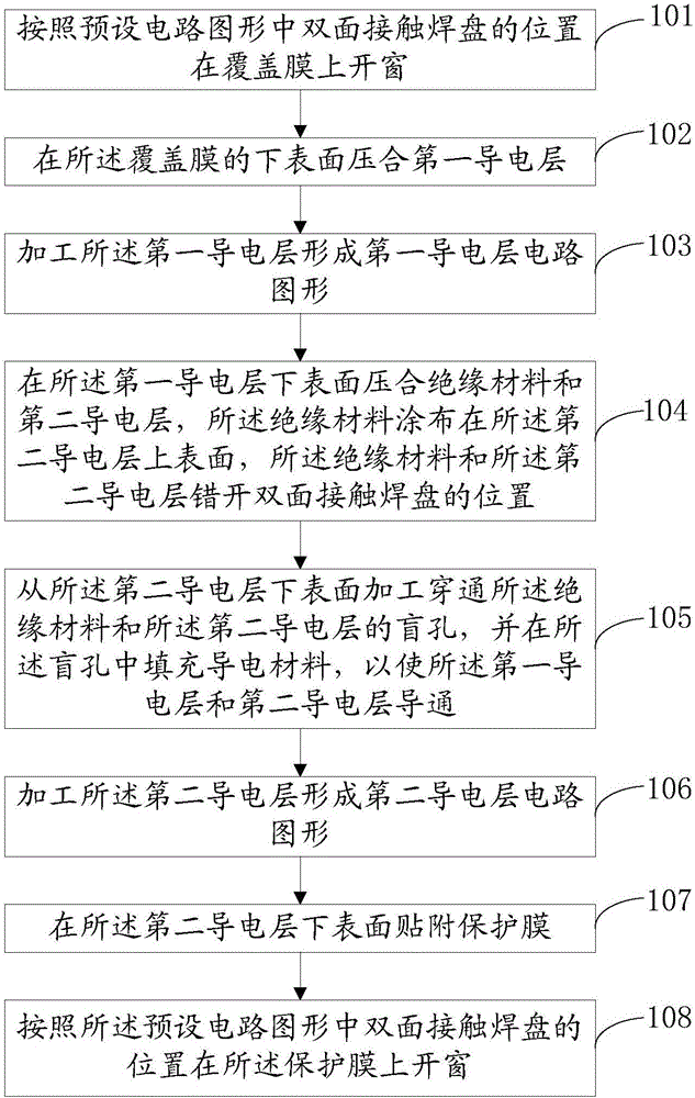
[0035] refer to figure 2 , shows a flow chart of a method for manufacturing a flexible circuit board in an embodiment of the present invention.

[0036] Step 101, opening windows on the cover film according to the positions of the double-sided contact pads in the preset circuit pattern.

[0037] In this embodiment, the cover film may include a polyimide film and a thermosetting adhesive coated on the polyimide film, and the cover film protects and insulates the wire circuit of the circuit board. According to the positions of the double-sided contact pads in the preset circuit pattern, windows are opened on the cover film. The window opening method can be at least one of laser processing window opening or mechanical mold punching window opening.

[0038] Step 102, pressing the first conductive layer on the lower surface of the covering film...

Embodiment 2

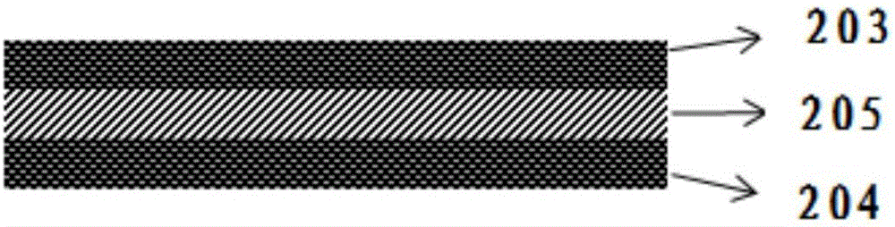
[0066] see Figure 3 to Figure 6 , a detailed introduction to a flexible circuit board provided by an embodiment of the present invention, the flexible circuit board includes:

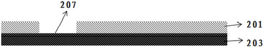
[0067] Covering film 201, protective film 202, first conductive layer 203, second conductive layer 204, insulating material 205, blind hole 206;

[0068] The cover film 201, the first conductive layer 203, the insulating material 205, the second conductive layer 204, and the protective film 202 are pressed from top to bottom to form the flexible circuit board;

[0069] The cover film 201 and the protective film 202 are opened at the position 207 of the double-sided contact pad in the preset circuit pattern;

[0070] The insulating material 205 and the second conductive layer 204 are pressed together with the first conductive layer by staggering the position 207 of the double-sided contact pad;

[0071] The insulating material 205 is coated on the upper surface of the second conductive layer 204;

[...


PUM


Abstract

The present invention provides a flexible printed circuit board and a manufacturing method thereof. The method comprises: performing windowing on a cover film according to the position of a two-sided contact bonding pad in a preset circuit pattern; performing press fit of a first conducting layer at the lower surface of the cover film; processing the first conducting layer to form a first conducting layer circuit pattern; performing press fit of insulation materials and a second conducting layer at the lower surface of the first conducting layer, wherein the upper surface of the second conducting layer is coated with the insulation materials, the insulation materials and the second conducting layer staggered with the position of the two-sided contact bonding pad; processing a blind hole punching through the insulation materials and the second conducting layer at the lower surface of the second conducting layer, and allowing the blind hole to be filled with conducting materials; processing the second conducting layer to form the second conducting layer circuit pattern; attaching a protective film to the lower surface of the second conducting layer; and performing windowing on the protective film according to the position of the two-sided contact bonding pad in the preset circuit pattern. The flexible printed circuit board is provided with a bonding pad which realizes two-sided contact and conduction through the first conducting layer so as to satisfy welding and conduction requirements and reduce the risk of the tearing of the bonding pad.

Description

technical field [0001] The invention relates to the field of circuit boards, in particular to a flexible circuit board and a manufacturing method thereof. Background technique [0002] FPC (Flexible Printed Circuit, flexible circuit board) is widely used in electronic products because of its softness and high reliability. According to the number of layers of circuit graphics, FPC can be divided into single-layer boards, double-layer boards and multi-layer boards. [0003] At present, FPC double-sided panels usually purchase double-sided flexible copper-clad laminates as the substrate, see figure 1 , to make circuits on the base material, the production process is as follows: Etch electrical circuits on double-sided flexible copper clad laminates, and then stick a cover film to protect the circuits. [0004] The circuit is made on the substrate, and the circuit forms a pad at the position where the window is opened in the cover film; but because there is an insulating layer...

Claims


Application Information

Patent Timeline
Patent Type & Authority Applications(China)
IPC IPC(8): H05K3/46H05K3/40H05K1/11
CPCH05K1/118H05K3/4007H05K3/4644H05K2201/05H05K2201/09372
Inventor 殷向兵谢长虹
Owner VIVO MOBILE COMM CO LTD
Why Eureka
Try Eureka